
User Manual
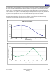
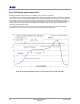
Table Of Contents
- 1 Introduction
- 2 Pin Configurations
- 3 CPU
- 4 Memory Organisation
- 5 System Clocks
- 6 Reset
- 7 Interrupt System
- 8 Wireless Transceiver
- 9 Digital Input/Output
- 10 Serial Peripheral Interface
- 11 Timers
- 12 Pulse Counters
- 13 Serial Communications
- 14 JTAG Debug Interface
- 15 Two-Wire Serial Interface
- 16 Four-Wire Digital Audio Interface
- 17 Random Number Generator
- 18 Sample FIFO
- 19 Intelligent Peripheral Interface
- 20 Analogue Peripherals
- 21 Power Management and Sleep Modes
- 22 Electrical Characteristics
- 22.1 Maximum Ratings
- 22.2 DC Electrical Characteristics
- 22.3 AC Characteristics
- 22.3.1 Reset and Voltage Brown-Out
- 22.3.2 SPI MasterTiming
- 22.3.3 Intelligent Peripheral (SPI Slave) Timing
- 22.3.4 Two-wire Serial Interface
- 22.3.5 Four-Wire Digital Audio Interface
- 22.3.6 Wakeup and Boot Load Timings
- 22.3.7 Bandgap Reference
- 22.3.8 Analogue to Digital Converters
- 22.3.9 Digital to Analogue Converters
- 22.3.10 Comparators
- 22.3.11 32kHz RC Oscillator
- 22.3.12 32kHz Crystal Oscillator
- 22.3.13 32MHz Crystal Oscillator
- 22.3.14 24MHz RC Oscillator
- 22.3.15 Temperature Sensor
- 22.3.16 Radio Transceiver
- Appendix A Mechanical and Ordering Information
- Appendix B Development Support

Jennic
94 JN-DS-JN5148-001 1v2 © Jennic 2009
Preliminary
B.4.2 PCB Design and Reflow Profile
PCB and land pattern designs are key to the reliability of any electronic circuit design.
The Institute for Interconnecting and Packaging Electronic Circuits (IPC) defines a number of standards for electronic
devices. One of these is the "Surface Mount Design and Land Pattern Standard" IPC-SM-782
[4], commonly referred
to as “IPC782". This specification defines the physical packaging characteristics and land patterns for a range of
surface mounted devices. IPC782 is also a useful reference document for general surface mount design techniques,
containing sections on design requirements, reliability and testability. Jennic strongly recommends that this be
referred to when designing the PCB.
The suggested reflow profile is shown in
Figure 56. The specific paste manufacturers guidelines on peak flow
temperature, soak times, time above liquidus and ramp rates should also be referenced.
Figure 56: Recommended Reflow Profile for Lead-free Solder Paste or PPF lead frame