
User Manual
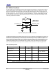
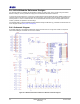
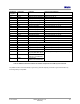
Table Of Contents
- 1 Introduction
- 2 Pin Configurations
- 3 CPU
- 4 Memory Organisation
- 5 System Clocks
- 6 Reset
- 7 Interrupt System
- 8 Wireless Transceiver
- 9 Digital Input/Output
- 10 Serial Peripheral Interface
- 11 Timers
- 12 Pulse Counters
- 13 Serial Communications
- 14 JTAG Debug Interface
- 15 Two-Wire Serial Interface
- 16 Four-Wire Digital Audio Interface
- 17 Random Number Generator
- 18 Sample FIFO
- 19 Intelligent Peripheral Interface
- 20 Analogue Peripherals
- 21 Power Management and Sleep Modes
- 22 Electrical Characteristics
- 22.1 Maximum Ratings
- 22.2 DC Electrical Characteristics
- 22.3 AC Characteristics
- 22.3.1 Reset and Voltage Brown-Out
- 22.3.2 SPI MasterTiming
- 22.3.3 Intelligent Peripheral (SPI Slave) Timing
- 22.3.4 Two-wire Serial Interface
- 22.3.5 Four-Wire Digital Audio Interface
- 22.3.6 Wakeup and Boot Load Timings
- 22.3.7 Bandgap Reference
- 22.3.8 Analogue to Digital Converters
- 22.3.9 Digital to Analogue Converters
- 22.3.10 Comparators
- 22.3.11 32kHz RC Oscillator
- 22.3.12 32kHz Crystal Oscillator
- 22.3.13 32MHz Crystal Oscillator
- 22.3.14 24MHz RC Oscillator
- 22.3.15 Temperature Sensor
- 22.3.16 Radio Transceiver
- Appendix A Mechanical and Ordering Information
- Appendix B Development Support

Jennic
© Jennic 2009 JN-DS-JN5148-001 1v2 93
Preliminary
Component
Designator
Value/Type Function PCB Layout Constraints
C13 10uF Power source decoupling
C14 100nF Analogue Power decoupling Adjacent to U1 pin 13
C16 100nF Digital power decoupling Adjacent to U1 pin 49
C15 100nF VB Synth decoupling Less than 5mm from U1 pin 10
C18 47pF VB Synth decoupling Less than 5mm from U1 pin 10
C2 10nF VB VCO decoupling Less than 5mm from U1 pin 12
C24 47pF VB VCO decoupling Less than 5mm from U1 pin 12
C3 100nF VB RF decoupling Less than 5mm from U1 pin 16 and U1 pin 18
C12 47pF VB RF decoupling Less than 5mm from U1 pin 16 and U1 pin 18
C8 100nF VB A decoupling Less than 5mm from U1 pin 27
C9 47pF VB A decoupling Less than 5mm from U1 pin 27
C6 100nF VB RAM decoupling Less than 5mm from U1 pin 35
C7 100nF VB Dig decoupling Less than 5mm from U1 pin 40
R1 43k I Bias Resistor Less than 5mm from U1 pin 14
C20 100nF Vref decoupling Less than 5mm from U1 pin 15
U2 4Mbit Serial Flash Memory (Numonyx M25P40A)
Y1 32MHz Crystal (Toyocom TSX 3225) (CL = 9pF, Max ESR 40R)
C10 15pF +/-5% COG Crystal Load Capacitor Adjacent to pin 8 and Y1 pin 1
C11 15pF +/-5% COG Crystal Load Capacitor Adjacent to pin 9 and Y1 pin 3
R2 Not fitted
C1 47pF AC Coupling
Phycomp 2238-869-15479
L1 5.6nH RF Matching Inductor
Johanson L-07C5N6SV6S
L2 2.7nH Load Inductor
MuRata LQP15MN2N7B02
Must be copied directly from the reference design.
Table 8: JN5148 Printed Antenna Reference Module Components and PCB Layout Constraints
The paddle should be connected directly to ground. Any pads that requiring connection to ground should do so by
connecting directly to the paddle.