
User Manual
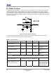
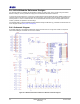
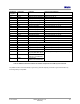
Table Of Contents
- 1 Introduction
- 2 Pin Configurations
- 3 CPU
- 4 Memory Organisation
- 5 System Clocks
- 6 Reset
- 7 Interrupt System
- 8 Wireless Transceiver
- 9 Digital Input/Output
- 10 Serial Peripheral Interface
- 11 Timers
- 12 Pulse Counters
- 13 Serial Communications
- 14 JTAG Debug Interface
- 15 Two-Wire Serial Interface
- 16 Four-Wire Digital Audio Interface
- 17 Random Number Generator
- 18 Sample FIFO
- 19 Intelligent Peripheral Interface
- 20 Analogue Peripherals
- 21 Power Management and Sleep Modes
- 22 Electrical Characteristics
- 22.1 Maximum Ratings
- 22.2 DC Electrical Characteristics
- 22.3 AC Characteristics
- 22.3.1 Reset and Voltage Brown-Out
- 22.3.2 SPI MasterTiming
- 22.3.3 Intelligent Peripheral (SPI Slave) Timing
- 22.3.4 Two-wire Serial Interface
- 22.3.5 Four-Wire Digital Audio Interface
- 22.3.6 Wakeup and Boot Load Timings
- 22.3.7 Bandgap Reference
- 22.3.8 Analogue to Digital Converters
- 22.3.9 Digital to Analogue Converters
- 22.3.10 Comparators
- 22.3.11 32kHz RC Oscillator
- 22.3.12 32kHz Crystal Oscillator
- 22.3.13 32MHz Crystal Oscillator
- 22.3.14 24MHz RC Oscillator
- 22.3.15 Temperature Sensor
- 22.3.16 Radio Transceiver
- Appendix A Mechanical and Ordering Information
- Appendix B Development Support

Jennic
92 JN-DS-JN5148-001 1v2 © Jennic 2009
Preliminary
B.4 JN5148 Module Reference Designs
For customers wishing to integrate the JN5148 device directly into their system, Jennic provide a range of Module
Reference Designs, covering standard and high-power modules fitted with different Antennae
To ensure the correct performance, it is strongly recommended that where possible the design details provided by the
reference designs, are used in their exact form for all end designs, this includes component values, pad dimensions,
track layouts etc. In order to minimise all risks, it is recommended that the entire layout of the appropriate reference
module, if possible, be replicated in the end design.
For full detail please consult the Standard Module Reference Design JN-RD-6001
[7] , available to download from the
Jennic Support web site
(www.jennic.com/support)
B.4.1 Schematic Diagram
A schematic diagram of the JN5148 PCB antenna reference module is shown in Figure 55. Details of component
values and PCB layout constraints can be found in
Table 8.
Figure 55: JN5148 Printed Antenna Reference Module Schematic Diagram