
User Manual
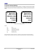
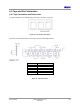
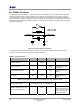
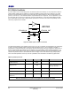
Table Of Contents
- 1 Introduction
- 2 Pin Configurations
- 3 CPU
- 4 Memory Organisation
- 5 System Clocks
- 6 Reset
- 7 Interrupt System
- 8 Wireless Transceiver
- 9 Digital Input/Output
- 10 Serial Peripheral Interface
- 11 Timers
- 12 Pulse Counters
- 13 Serial Communications
- 14 JTAG Debug Interface
- 15 Two-Wire Serial Interface
- 16 Four-Wire Digital Audio Interface
- 17 Random Number Generator
- 18 Sample FIFO
- 19 Intelligent Peripheral Interface
- 20 Analogue Peripherals
- 21 Power Management and Sleep Modes
- 22 Electrical Characteristics
- 22.1 Maximum Ratings
- 22.2 DC Electrical Characteristics
- 22.3 AC Characteristics
- 22.3.1 Reset and Voltage Brown-Out
- 22.3.2 SPI MasterTiming
- 22.3.3 Intelligent Peripheral (SPI Slave) Timing
- 22.3.4 Two-wire Serial Interface
- 22.3.5 Four-Wire Digital Audio Interface
- 22.3.6 Wakeup and Boot Load Timings
- 22.3.7 Bandgap Reference
- 22.3.8 Analogue to Digital Converters
- 22.3.9 Digital to Analogue Converters
- 22.3.10 Comparators
- 22.3.11 32kHz RC Oscillator
- 22.3.12 32kHz Crystal Oscillator
- 22.3.13 32MHz Crystal Oscillator
- 22.3.14 24MHz RC Oscillator
- 22.3.15 Temperature Sensor
- 22.3.16 Radio Transceiver
- Appendix A Mechanical and Ordering Information
- Appendix B Development Support

Jennic
86 JN-DS-JN5148-001 1v2 © Jennic 2009
Preliminary
Appendix B Development Support
B.1 Crystal Oscillators
This section covers some of the general background to crystal oscillators, to help the user make informed decisions
concerning the choice of crystal and the associated capacitors.
B.1.1 Crystal Equivalent Circuit
Cs
Lm
Cm
Rm
C2C1
Where
mC is the motional capacitance
mL is the motional inductance. This together with mC defines the oscillation frequency (series)
mR is the equivalent series resistance ( ESR ).
SC is the shunt or package capacitance and this is a parasitic
B.1.2 Crystal Load Capacitance
The crystal load capacitance is the total capacitance seen at the crystal pins, from all sources. As the load
capacitance (CL) affects the oscillation frequency by a process known as ‘pulling’, crystal manufacturers specify the
frequency for a given load capacitance only. A typical pulling coefficient is 15ppm/pF, to put this into context the
maximum frequency error in the IEEE802.15.4 specification is +/-40ppm for the transmitted signal. Therefore, it is
important for resonance at 32MHz exactly, that the specified load capacitance is provided.
The load capacitance can be calculated using:
CL =
21
21
TT
TT
CC
CC
+
×
Total capacitance
inPT CCCC 1111
+
+
=
Where
1C is the capacitor component
PC1 is the PCB parasitic capacitance. With the recommended layout this is about 1.6pF
inC1 is the on-chip parasitic capacitance and is about 1.4pF typically.
Similarly for
2TC
Hence for a 9pF load capacitance, and a tight layout the external capacitors should be 15pF