
User Manual
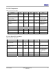
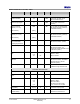
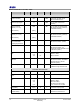
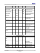
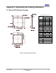
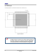
Table Of Contents
- 1 Introduction
- 2 Pin Configurations
- 3 CPU
- 4 Memory Organisation
- 5 System Clocks
- 6 Reset
- 7 Interrupt System
- 8 Wireless Transceiver
- 9 Digital Input/Output
- 10 Serial Peripheral Interface
- 11 Timers
- 12 Pulse Counters
- 13 Serial Communications
- 14 JTAG Debug Interface
- 15 Two-Wire Serial Interface
- 16 Four-Wire Digital Audio Interface
- 17 Random Number Generator
- 18 Sample FIFO
- 19 Intelligent Peripheral Interface
- 20 Analogue Peripherals
- 21 Power Management and Sleep Modes
- 22 Electrical Characteristics
- 22.1 Maximum Ratings
- 22.2 DC Electrical Characteristics
- 22.3 AC Characteristics
- 22.3.1 Reset and Voltage Brown-Out
- 22.3.2 SPI MasterTiming
- 22.3.3 Intelligent Peripheral (SPI Slave) Timing
- 22.3.4 Two-wire Serial Interface
- 22.3.5 Four-Wire Digital Audio Interface
- 22.3.6 Wakeup and Boot Load Timings
- 22.3.7 Bandgap Reference
- 22.3.8 Analogue to Digital Converters
- 22.3.9 Digital to Analogue Converters
- 22.3.10 Comparators
- 22.3.11 32kHz RC Oscillator
- 22.3.12 32kHz Crystal Oscillator
- 22.3.13 32MHz Crystal Oscillator
- 22.3.14 24MHz RC Oscillator
- 22.3.15 Temperature Sensor
- 22.3.16 Radio Transceiver
- Appendix A Mechanical and Ordering Information
- Appendix B Development Support

Jennic
© Jennic 2009 JN-DS-JN5148-001 1v2 79
Preliminary
Appendix A Mechanical and Ordering Information
A.1 56-pin QFN Package Drawing
Figure 47: 56-pin QFN Package Drawings
Controlling Dimension: mm
millimetres
Symbol
Min. Nom. Max.
A ------ ------ 0.9
A1 0.00 0.01 0.05
A2 ------ 0.65 0.7
A3 0.20 Ref.
b 0.2 0.25 0.3
D 8.00 bsc
D1 7.75 bsc
D2 6.20 6.40 6.60
E 8.00 bsc
E1 7.75 bsc
E2 6.20 6.40 6.60
L 0.30 0.40 0.50
e 0.50 bsc
υ1
0° ------ 12°
R 0.09 ------ ------
Tolerances of Form and Position
aaa 0.10
bbb 0.10
ccc 0.05