
User Manual
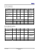
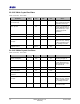
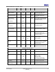
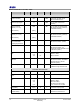
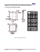
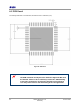
Table Of Contents
- 1 Introduction
- 2 Pin Configurations
- 3 CPU
- 4 Memory Organisation
- 5 System Clocks
- 6 Reset
- 7 Interrupt System
- 8 Wireless Transceiver
- 9 Digital Input/Output
- 10 Serial Peripheral Interface
- 11 Timers
- 12 Pulse Counters
- 13 Serial Communications
- 14 JTAG Debug Interface
- 15 Two-Wire Serial Interface
- 16 Four-Wire Digital Audio Interface
- 17 Random Number Generator
- 18 Sample FIFO
- 19 Intelligent Peripheral Interface
- 20 Analogue Peripherals
- 21 Power Management and Sleep Modes
- 22 Electrical Characteristics
- 22.1 Maximum Ratings
- 22.2 DC Electrical Characteristics
- 22.3 AC Characteristics
- 22.3.1 Reset and Voltage Brown-Out
- 22.3.2 SPI MasterTiming
- 22.3.3 Intelligent Peripheral (SPI Slave) Timing
- 22.3.4 Two-wire Serial Interface
- 22.3.5 Four-Wire Digital Audio Interface
- 22.3.6 Wakeup and Boot Load Timings
- 22.3.7 Bandgap Reference
- 22.3.8 Analogue to Digital Converters
- 22.3.9 Digital to Analogue Converters
- 22.3.10 Comparators
- 22.3.11 32kHz RC Oscillator
- 22.3.12 32kHz Crystal Oscillator
- 22.3.13 32MHz Crystal Oscillator
- 22.3.14 24MHz RC Oscillator
- 22.3.15 Temperature Sensor
- 22.3.16 Radio Transceiver
- Appendix A Mechanical and Ordering Information
- Appendix B Development Support

Jennic
© Jennic 2009 JN-DS-JN5148-001 1v2 73
Preliminary
22.3.14 24MHz RC Oscillator
VDD = 2.0 to 3.6V, -40 to +85ºC
Parameter Min Typ Max Unit Notes
Current consumption of cell 160 µA
Clock native accuracy -22% 24MHz +28%
Calibrated centre frequency
accuracy
-7% 24MHz +7%
Variation with temperature -0.015 %/°C
Variation with VDD2 0.15 %/V
Startup time 1 us
22.3.15 Temperature Sensor
VDD = 2.0 to 3.6V, -40 to +85ºC
Parameter Min Typ Max Unit Notes
Operating Range -40 - 85
°C
Sensor Gain -1.44 -1.55 -1.66
mV/°C
Accuracy - -
±10 °C
Non-linearity - - 2.5
°C
Output Voltage 630 855 mV Includes absolute variation
due to manufacturing & temp
Typical Voltage 745 mV
Typical at 3.0V 25°C
Resolution 0.154 0.182 0.209
°C/LSB
0 to Vref ADC I/P Range