
User Manual
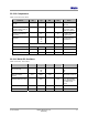
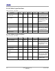
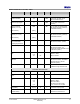
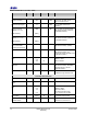
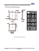
Table Of Contents
- 1 Introduction
- 2 Pin Configurations
- 3 CPU
- 4 Memory Organisation
- 5 System Clocks
- 6 Reset
- 7 Interrupt System
- 8 Wireless Transceiver
- 9 Digital Input/Output
- 10 Serial Peripheral Interface
- 11 Timers
- 12 Pulse Counters
- 13 Serial Communications
- 14 JTAG Debug Interface
- 15 Two-Wire Serial Interface
- 16 Four-Wire Digital Audio Interface
- 17 Random Number Generator
- 18 Sample FIFO
- 19 Intelligent Peripheral Interface
- 20 Analogue Peripherals
- 21 Power Management and Sleep Modes
- 22 Electrical Characteristics
- 22.1 Maximum Ratings
- 22.2 DC Electrical Characteristics
- 22.3 AC Characteristics
- 22.3.1 Reset and Voltage Brown-Out
- 22.3.2 SPI MasterTiming
- 22.3.3 Intelligent Peripheral (SPI Slave) Timing
- 22.3.4 Two-wire Serial Interface
- 22.3.5 Four-Wire Digital Audio Interface
- 22.3.6 Wakeup and Boot Load Timings
- 22.3.7 Bandgap Reference
- 22.3.8 Analogue to Digital Converters
- 22.3.9 Digital to Analogue Converters
- 22.3.10 Comparators
- 22.3.11 32kHz RC Oscillator
- 22.3.12 32kHz Crystal Oscillator
- 22.3.13 32MHz Crystal Oscillator
- 22.3.14 24MHz RC Oscillator
- 22.3.15 Temperature Sensor
- 22.3.16 Radio Transceiver
- Appendix A Mechanical and Ordering Information
- Appendix B Development Support

Jennic
© Jennic 2009 JN-DS-JN5148-001 1v2 71
Preliminary
22.3.10 Comparators
VDD = 2.0 to 3.6V -40 to +85ºC
Parameter Min Typ Max Unit Notes
Analogue response time
(normal)
80 125 ns +/- 250mV overdrive
10pF load
Total response time
(normal) including delay to
Interrupt controller
105 + 125 ns Digital delay can be
up to a max. of two
16MHz clock periods
Analogue response time
(low power)
2.4
µs +/- 250mV overdrive
No digital delay
Hysteresis 10
20
40
mV Programmable in 3
steps and zero
Vref (Internal) See Section 22.3.7 Bandgap Reference V
Common Mode input range 0 Vdd V
Current (normal mode) 73 µA
Current (low power mode) 0.8 µA
22.3.11 32kHz RC Oscillator
VDD = 2.0 to 3.6V, -40 to +85 ºC
Parameter Min Typ Max Unit Notes
Current consumption of cell
and counter logic
1.45
1.25
1.05
µA 3.6V
3.0V
2.0v
32kHz clock native
accuracy
-30% 32kHz +30%
Typical is at 3.0V 25°C
Calibrated 32kHz accuracy ±250 ppm For a 1 second sleep
period calibrating over
20 x 32kHz clock
periods
Variation with temperature -0.010 %/°C
Variation with VDD2 -1.1 %/V