
User Manual
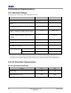
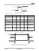


Table Of Contents
- 1 Introduction
- 2 Pin Configurations
- 3 CPU
- 4 Memory Organisation
- 5 System Clocks
- 6 Reset
- 7 Interrupt System
- 8 Wireless Transceiver
- 9 Digital Input/Output
- 10 Serial Peripheral Interface
- 11 Timers
- 12 Pulse Counters
- 13 Serial Communications
- 14 JTAG Debug Interface
- 15 Two-Wire Serial Interface
- 16 Four-Wire Digital Audio Interface
- 17 Random Number Generator
- 18 Sample FIFO
- 19 Intelligent Peripheral Interface
- 20 Analogue Peripherals
- 21 Power Management and Sleep Modes
- 22 Electrical Characteristics
- 22.1 Maximum Ratings
- 22.2 DC Electrical Characteristics
- 22.3 AC Characteristics
- 22.3.1 Reset and Voltage Brown-Out
- 22.3.2 SPI MasterTiming
- 22.3.3 Intelligent Peripheral (SPI Slave) Timing
- 22.3.4 Two-wire Serial Interface
- 22.3.5 Four-Wire Digital Audio Interface
- 22.3.6 Wakeup and Boot Load Timings
- 22.3.7 Bandgap Reference
- 22.3.8 Analogue to Digital Converters
- 22.3.9 Digital to Analogue Converters
- 22.3.10 Comparators
- 22.3.11 32kHz RC Oscillator
- 22.3.12 32kHz Crystal Oscillator
- 22.3.13 32MHz Crystal Oscillator
- 22.3.14 24MHz RC Oscillator
- 22.3.15 Temperature Sensor
- 22.3.16 Radio Transceiver
- Appendix A Mechanical and Ordering Information
- Appendix B Development Support

Jennic
70 JN-DS-JN5148-001 1v2 © Jennic 2009
Preliminary
22.3.9 Digital to Analogue Converters
VDD = 3.0V, VREF = 1.2V, -40 to +85ºC
Parameter Min Typ Max Unit Notes
Resolution 12 bits
Current consumption 215 (single)
235 (both)
µA
Integral nonlinearity ± 2 LSB
Differential nonlinearity -1 +1 LSB Guaranteed monotonic
Offset error ± 10 mV
Gain error ± 10 mV
Internal clock 2MHz,
1MHz,
500kHz,
250kHz
16MHz input clock,
programmable
prescaler
Output settling time to
0.5LSB
5 µs With 10k ohms & 20pF
load
Minimum Update time 10 µs 2MHz Clock with
sample period of 2
Output voltage swing 0 Lower of Vdd-1.2 and Vref V Output voltage swing
Gain =0
Output voltage swing 0 Lower of 2x(Vdd-1.2 ) and
Vdd-0.2 and 2xVref
V Output voltage swing
Gain =1
Vref (Internal) See Section 22.3.7 Bandgap Reference
VREF (External) 0.8 1.2 1.6 V Allowable range into
VREF pin
Resistive load 10 kΩ To ground
Capacitive load 20 pF
Digital input coding Binary