
User Manual
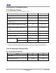
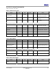
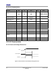
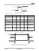
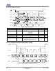

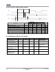

Table Of Contents
- 1 Introduction
- 2 Pin Configurations
- 3 CPU
- 4 Memory Organisation
- 5 System Clocks
- 6 Reset
- 7 Interrupt System
- 8 Wireless Transceiver
- 9 Digital Input/Output
- 10 Serial Peripheral Interface
- 11 Timers
- 12 Pulse Counters
- 13 Serial Communications
- 14 JTAG Debug Interface
- 15 Two-Wire Serial Interface
- 16 Four-Wire Digital Audio Interface
- 17 Random Number Generator
- 18 Sample FIFO
- 19 Intelligent Peripheral Interface
- 20 Analogue Peripherals
- 21 Power Management and Sleep Modes
- 22 Electrical Characteristics
- 22.1 Maximum Ratings
- 22.2 DC Electrical Characteristics
- 22.3 AC Characteristics
- 22.3.1 Reset and Voltage Brown-Out
- 22.3.2 SPI MasterTiming
- 22.3.3 Intelligent Peripheral (SPI Slave) Timing
- 22.3.4 Two-wire Serial Interface
- 22.3.5 Four-Wire Digital Audio Interface
- 22.3.6 Wakeup and Boot Load Timings
- 22.3.7 Bandgap Reference
- 22.3.8 Analogue to Digital Converters
- 22.3.9 Digital to Analogue Converters
- 22.3.10 Comparators
- 22.3.11 32kHz RC Oscillator
- 22.3.12 32kHz Crystal Oscillator
- 22.3.13 32MHz Crystal Oscillator
- 22.3.14 24MHz RC Oscillator
- 22.3.15 Temperature Sensor
- 22.3.16 Radio Transceiver
- Appendix A Mechanical and Ordering Information
- Appendix B Development Support

Jennic
© Jennic 2009 JN-DS-JN5148-001 1v2 67
Preliminary
Parameter Symbol Min Max Unit
Clock period t
ck
125.0 - ns
Data setup time t
si
15 - ns
Data hold time t
hi
15 ns
Data invalid period t
vo
- 40 ns
Select set-up period t
sss
15 - ns
Select hold period t
ssh
15 - ns
Select asserted to output data driven t
lz
20 ns
Select negated to data output tri-stated t
hz
20 ns
22.3.4 Two-wire Serial Interface
t
BUF
Sr P SS
t
LOW
t
HD;STA
t
F
t
R
t
HD;DAT
t
HIGH
t
SU;DAT
t
SU;STA
t
HD;STA
t
SU;STO
t
SP
t
R
t
F
SIF_D
SIF_CLK
Figure 46: Two-wire Serial Interface Timing
Standard Mode Fast Mode
Parameter Symbol
Min Max Min Max
Unit
SIF_CLK clock frequency
f
SCL
0 100 0 400 kHz
Hold time (repeated) START condition.
After this period, the first clock pulse is
generated
t
HD:STA
4 - 0.6 - µs
LOW period of the SIF_CLK clock
t
LOW
4.7 - 1.3 - µs
HIGH period of the SIF_CLK clock
t
HIGH
4 - 0.6 - µs
Set-up time for repeated START condition t
SU:STA
4.7 - 0.6 - µs
Data setup time SIF_D t
SU:DAT
0.25 - 0.1 - µs
Rise Time SIF_D and SIF_CLK t
R
- 1000 20+0.1Cb 300 ns
Fall Time SIF_D and SIF_CLK t
F
- 300 20+0.1Cb 300 ns
Set-up time for STOP condition t
SU:STO
4 - 0.6 - µs
Bus free time between a STOP and START
condition
t
BUF
4.7 - 1.3 - µs
Pulse width of spikes that will be
suppressed by input filters (Note 1)
t
SP
- 60 - 60 ns
Capacitive load for each bus line C
b
- 400 - 400 pF
Noise margin at the LOW level for each
connected device (including hysteresis)
V
nl
0.1VDD - 0.1VDD - V
Noise margin at the HIGH level for each
connected device (including hysteresis)
V
nh
0.2VDD - 0.2VDD - V
Note 1: This figure indicates the pulse width that is guaranteed to be suppressed. Pulse with widths up to 125nsec
may alos get suppressed.