
User Manual
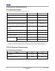
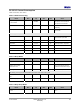
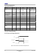


Table Of Contents
- 1 Introduction
- 2 Pin Configurations
- 3 CPU
- 4 Memory Organisation
- 5 System Clocks
- 6 Reset
- 7 Interrupt System
- 8 Wireless Transceiver
- 9 Digital Input/Output
- 10 Serial Peripheral Interface
- 11 Timers
- 12 Pulse Counters
- 13 Serial Communications
- 14 JTAG Debug Interface
- 15 Two-Wire Serial Interface
- 16 Four-Wire Digital Audio Interface
- 17 Random Number Generator
- 18 Sample FIFO
- 19 Intelligent Peripheral Interface
- 20 Analogue Peripherals
- 21 Power Management and Sleep Modes
- 22 Electrical Characteristics
- 22.1 Maximum Ratings
- 22.2 DC Electrical Characteristics
- 22.3 AC Characteristics
- 22.3.1 Reset and Voltage Brown-Out
- 22.3.2 SPI MasterTiming
- 22.3.3 Intelligent Peripheral (SPI Slave) Timing
- 22.3.4 Two-wire Serial Interface
- 22.3.5 Four-Wire Digital Audio Interface
- 22.3.6 Wakeup and Boot Load Timings
- 22.3.7 Bandgap Reference
- 22.3.8 Analogue to Digital Converters
- 22.3.9 Digital to Analogue Converters
- 22.3.10 Comparators
- 22.3.11 32kHz RC Oscillator
- 22.3.12 32kHz Crystal Oscillator
- 22.3.13 32MHz Crystal Oscillator
- 22.3.14 24MHz RC Oscillator
- 22.3.15 Temperature Sensor
- 22.3.16 Radio Transceiver
- Appendix A Mechanical and Ordering Information
- Appendix B Development Support

Jennic
© Jennic 2009 JN-DS-JN5148-001 1v2 65
Preliminary
Internal RESET
RESETN
V
RST
t
STAB
t
RST
Figure 42: Externally Applied Reset
VDD = 2.0 to 3.6V, -40 to +85º C
Parameter Min Typ Max Unit Notes
External Reset pulse width
to initiate reset sequence
(t
RST
)
1
µs
Assumes internal pullup
resistor value of 100K
worst case and ~5pF
external capacitance
External Reset threshold
voltage (V
RST
)
VDD2 x 0.7 V Minimum voltage to
avoid being reset
Internal Power-on Reset
threshold voltage (V
POT
)
1.47
1.42
V Rising
Falling
Reset stabilisation time
(t
STAB
)
0.84 ms Note 1
Brown-out Threshold
Voltage (V
TH
)
1.95
2.25
2.65
2.95
V Configurable threshold
with 4 levels
Brown-out Hysteresis
(V
HYS
)
45
60
85
100
mV Corresponding to the 4
threshold levels
1
Time from release of reset to start of executing ROM code. Loading program from Flash occurs in addition to this.
VTH + VHYS
VTH
DVDD
Internal POR
Internal BOReset
VPOT
Figure 43: Power on Reset followed by Brown-out Detect