
User Manual
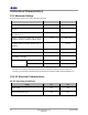
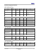
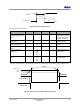


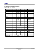
Table Of Contents
- 1 Introduction
- 2 Pin Configurations
- 3 CPU
- 4 Memory Organisation
- 5 System Clocks
- 6 Reset
- 7 Interrupt System
- 8 Wireless Transceiver
- 9 Digital Input/Output
- 10 Serial Peripheral Interface
- 11 Timers
- 12 Pulse Counters
- 13 Serial Communications
- 14 JTAG Debug Interface
- 15 Two-Wire Serial Interface
- 16 Four-Wire Digital Audio Interface
- 17 Random Number Generator
- 18 Sample FIFO
- 19 Intelligent Peripheral Interface
- 20 Analogue Peripherals
- 21 Power Management and Sleep Modes
- 22 Electrical Characteristics
- 22.1 Maximum Ratings
- 22.2 DC Electrical Characteristics
- 22.3 AC Characteristics
- 22.3.1 Reset and Voltage Brown-Out
- 22.3.2 SPI MasterTiming
- 22.3.3 Intelligent Peripheral (SPI Slave) Timing
- 22.3.4 Two-wire Serial Interface
- 22.3.5 Four-Wire Digital Audio Interface
- 22.3.6 Wakeup and Boot Load Timings
- 22.3.7 Bandgap Reference
- 22.3.8 Analogue to Digital Converters
- 22.3.9 Digital to Analogue Converters
- 22.3.10 Comparators
- 22.3.11 32kHz RC Oscillator
- 22.3.12 32kHz Crystal Oscillator
- 22.3.13 32MHz Crystal Oscillator
- 22.3.14 24MHz RC Oscillator
- 22.3.15 Temperature Sensor
- 22.3.16 Radio Transceiver
- Appendix A Mechanical and Ordering Information
- Appendix B Development Support

Jennic
62 JN-DS-JN5148-001 1v2 © Jennic 2009
Preliminary
22 Electrical Characteristics
22.1 Maximum Ratings
Exceeding these conditions may result in damage to the device.
Parameter Min Max
Device supply voltage VDD1, VDD2 -0.3V 3.6V
Supply voltage at voltage regulator bypass pins
VB_xxx
-0.3V 1.98V
Voltage on analogue pins XTALOUT, XTALIN,
VCOTUNE, RF_IN.
-0.3V VB_xxx + 0.3V
Voltage on analogue pins VREF, ADC1-4, DAC1-2,
COMP1M, COMP1P, COMP2M, COMP2P, IBIAS
-0.3V VDD1 + 0.3V
Voltage on 5v tolerant digital pins SPICLK,
SPIMOSI, SPIMISO, SPISEL0, DIO08 & DIO11-19,
RESETN
-0.3V Lower of (VDD2 + 2V)
and 5.5V
Voltage on 3v tolerant digital pins DIO9, DIO10 -0.3V VDD2 + 0.3V
Storage temperature -40ºC 150ºC
Reflow soldering temperature according to
IPC/JEDEC J-STD-020C
260ºC
Human Body Model
1
2.0kV ESD rating
4
Charged Device Model
2
500V
1) Testing for Human Body Model discharge is performed as specified in JEDEC Standard JESD22-A114.
2) Testing for Charged Device Model discharge is performed as specified in JEDEC Standard JESD22-C101.
22.2 DC Electrical Characteristics
22.2.1 Operating Conditions
Supply Min Max
VDD1, VDD2 2.0V 3.6V
Ambient temperature range -40ºC 85ºC