
User Manual
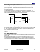
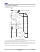
Table Of Contents
- 1 Introduction
- 2 Pin Configurations
- 3 CPU
- 4 Memory Organisation
- 5 System Clocks
- 6 Reset
- 7 Interrupt System
- 8 Wireless Transceiver
- 9 Digital Input/Output
- 10 Serial Peripheral Interface
- 11 Timers
- 12 Pulse Counters
- 13 Serial Communications
- 14 JTAG Debug Interface
- 15 Two-Wire Serial Interface
- 16 Four-Wire Digital Audio Interface
- 17 Random Number Generator
- 18 Sample FIFO
- 19 Intelligent Peripheral Interface
- 20 Analogue Peripherals
- 21 Power Management and Sleep Modes
- 22 Electrical Characteristics
- 22.1 Maximum Ratings
- 22.2 DC Electrical Characteristics
- 22.3 AC Characteristics
- 22.3.1 Reset and Voltage Brown-Out
- 22.3.2 SPI MasterTiming
- 22.3.3 Intelligent Peripheral (SPI Slave) Timing
- 22.3.4 Two-wire Serial Interface
- 22.3.5 Four-Wire Digital Audio Interface
- 22.3.6 Wakeup and Boot Load Timings
- 22.3.7 Bandgap Reference
- 22.3.8 Analogue to Digital Converters
- 22.3.9 Digital to Analogue Converters
- 22.3.10 Comparators
- 22.3.11 32kHz RC Oscillator
- 22.3.12 32kHz Crystal Oscillator
- 22.3.13 32MHz Crystal Oscillator
- 22.3.14 24MHz RC Oscillator
- 22.3.15 Temperature Sensor
- 22.3.16 Radio Transceiver
- Appendix A Mechanical and Ordering Information
- Appendix B Development Support

Jennic
60 JN-DS-JN5148-001 1v2 © Jennic 2009
Preliminary
21 Power Management and Sleep Modes
21.1 Operating Modes
Three operating modes are provided in the JN5148 that enable the system power consumption to be controlled
carefully to maximise battery life.
•
Active Processing Mode
• Sleep Mode
•
Deep Sleep Mode
The variation in power consumption of the three modes is a result of having a series of power domains within the chip
that may be controllably powered on or off.
21.1.1 Power Domains
The JN5148 has the following power domains:
• VDD Supply Domain: supplies the wake-up timers and controller, DIO blocks, Comparators, 32kHz RC and
crystal oscillators. This domain is driven from the external supply (battery) and is always powered. The wake-up
timers and controller, and the 32kHz RC and crystal oscillators may be powered on or off in sleep mode through
software control.
• Digital Logic Domain: supplies the digital peripherals, CPU, ROM, Baseband controller, Modem and Encryption
processor. It is powered off during sleep mode.
• Analogue Domain: supplies the ADC, DACs and the temperature sensor. It is powered off during sleep mode
and may be powered on or off in active processing mode through software control.
• RAM Domain: supplies the RAM during sleep mode to retain the memory contents. It may be powered on or off
for sleep mode through software control.
• Radio Domain: supplies the radio interface. It is powered during transmit and receive and controlled by the
baseband processor. It is powered off during sleep mode.
The current consumption figures for the different modes of operation of the device is given in section
22.2.2.
21.2 Active Processing Mode
Active processing mode in the JN5148 is where all of the application processing takes place. By default, the CPU will
execute at the selected clock speed executing application firmware. All of the peripherals are available to the
application, as are options to actively enable or disable them to control power consumption; see specific peripheral
sections for details.
Whilst in Active processing mode there is the option to doze the CPU but keep the rest of the chip active; this is
particularly useful for radio transmit and receive operations, where the CPU operation is not required therefore saving
power.
21.2.1 CPU Doze
Whilst in doze mode, CPU operation is stopped but the chip remains powered and the digital peripherals continue to
run. Doze mode is entered through software and is terminated by any interrupt request. Once the interrupt service
routine has been executed, normal program execution resumes. Doze mode uses more power than sleep and deep
sleep modes but requires less time to restart and can therefore be used as a low power alternative to an idle loop.
Whilst in CPU doze the current associated with the CPU is not consumed, therefore the basic device current is
reduced as shown in the figures in section
22.2.2.1.
21.3 Sleep Mode
The JN5148 enters sleep mode through software control. In this mode most of the internal chip functions are
shutdown to save power, however the state of DIO pins are retained, including the output values and pull-up enables,