
User Manual
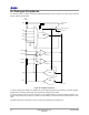
Table Of Contents
- 1 Introduction
- 2 Pin Configurations
- 3 CPU
- 4 Memory Organisation
- 5 System Clocks
- 6 Reset
- 7 Interrupt System
- 8 Wireless Transceiver
- 9 Digital Input/Output
- 10 Serial Peripheral Interface
- 11 Timers
- 12 Pulse Counters
- 13 Serial Communications
- 14 JTAG Debug Interface
- 15 Two-Wire Serial Interface
- 16 Four-Wire Digital Audio Interface
- 17 Random Number Generator
- 18 Sample FIFO
- 19 Intelligent Peripheral Interface
- 20 Analogue Peripherals
- 21 Power Management and Sleep Modes
- 22 Electrical Characteristics
- 22.1 Maximum Ratings
- 22.2 DC Electrical Characteristics
- 22.3 AC Characteristics
- 22.3.1 Reset and Voltage Brown-Out
- 22.3.2 SPI MasterTiming
- 22.3.3 Intelligent Peripheral (SPI Slave) Timing
- 22.3.4 Two-wire Serial Interface
- 22.3.5 Four-Wire Digital Audio Interface
- 22.3.6 Wakeup and Boot Load Timings
- 22.3.7 Bandgap Reference
- 22.3.8 Analogue to Digital Converters
- 22.3.9 Digital to Analogue Converters
- 22.3.10 Comparators
- 22.3.11 32kHz RC Oscillator
- 22.3.12 32kHz Crystal Oscillator
- 22.3.13 32MHz Crystal Oscillator
- 22.3.14 24MHz RC Oscillator
- 22.3.15 Temperature Sensor
- 22.3.16 Radio Transceiver
- Appendix A Mechanical and Ordering Information
- Appendix B Development Support

Jennic
© Jennic 2009 JN-DS-JN5148-001 1v2 59
Preliminary
20.3 Comparators
The JN5148 contains two analogue comparators COMP1 and COMP2 that are designed to have true rail-to-rail
inputs and operate over the full voltage range of the analogue supply VDD1. The hysteresis level (common to both
comparators) can be set to a nominal value of 0mV, 10mV, 20mV or 40mV. In addition, the source of the negative
input signal for each comparator (COMP1M and COMP2M) can be set to the internal voltage reference, the output of
DAC1 or DAC2 (COMP1 or COMP2 respectively) or the appropriate external pin. The comparator outputs are routed
to internal registers and can be polled, or can be used to generate interrupts. The comparators can be disabled to
reduce power consumption.
The comparators have a low power mode where the response time of the comparator is slower than normal and is
specified in section
22.3.10. This mode may be used during non-sleep operation however it is particularly useful in
sleep mode to wake up the JN5148 from sleep where low current consumption is important. The wakeup action and
the configuration for which edge of the comparator output will be active are controlled through software. In sleep
mode the negative input signal source, must be configured to be driven from the external pins.