
User Manual
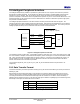
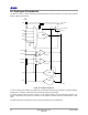
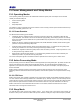
Table Of Contents
- 1 Introduction
- 2 Pin Configurations
- 3 CPU
- 4 Memory Organisation
- 5 System Clocks
- 6 Reset
- 7 Interrupt System
- 8 Wireless Transceiver
- 9 Digital Input/Output
- 10 Serial Peripheral Interface
- 11 Timers
- 12 Pulse Counters
- 13 Serial Communications
- 14 JTAG Debug Interface
- 15 Two-Wire Serial Interface
- 16 Four-Wire Digital Audio Interface
- 17 Random Number Generator
- 18 Sample FIFO
- 19 Intelligent Peripheral Interface
- 20 Analogue Peripherals
- 21 Power Management and Sleep Modes
- 22 Electrical Characteristics
- 22.1 Maximum Ratings
- 22.2 DC Electrical Characteristics
- 22.3 AC Characteristics
- 22.3.1 Reset and Voltage Brown-Out
- 22.3.2 SPI MasterTiming
- 22.3.3 Intelligent Peripheral (SPI Slave) Timing
- 22.3.4 Two-wire Serial Interface
- 22.3.5 Four-Wire Digital Audio Interface
- 22.3.6 Wakeup and Boot Load Timings
- 22.3.7 Bandgap Reference
- 22.3.8 Analogue to Digital Converters
- 22.3.9 Digital to Analogue Converters
- 22.3.10 Comparators
- 22.3.11 32kHz RC Oscillator
- 22.3.12 32kHz Crystal Oscillator
- 22.3.13 32MHz Crystal Oscillator
- 22.3.14 24MHz RC Oscillator
- 22.3.15 Temperature Sensor
- 22.3.16 Radio Transceiver
- Appendix A Mechanical and Ordering Information
- Appendix B Development Support

Jennic
56 JN-DS-JN5148-001 1v2 © Jennic 2009
Preliminary
20 Analogue Peripherals
The JN5148 contains a number of analogue peripherals allowing the direct connection of a wide range of external
sensors, switches and actuators.
ADC
DAC1
DAC2
VREF
Chip
Boundary
Internal Reference
Processor Bus
Supply Voltage
(VDD1)
Vref select
Temp
Sensor
Comparator 2
Comparator 1
COMP2M
COMP1M
COMP1P
COMP2P
DAC1
DAC2
ADC1
ADC2
ADC3
ADC4
Vref
Figure 39: Analogue Peripherals
In order to provide good isolation from digital noise, the analogue peripherals are powered by a separate regulator,
supplied from the analogue supply VDD1 and referenced to analogue ground VSSA.
A common reference Vref for the ADC and DAC can be selected between an internal bandgap reference or an
external voltage reference supplied to the VREF pin. Gain settings for the ADC and DAC are independent of each
other.
The ADC and DAC are clocked from a common clock source derived from the 16MHz clock