
User Manual
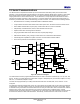
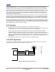
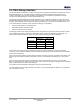
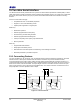
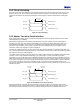
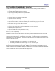
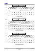
Table Of Contents
- 1 Introduction
- 2 Pin Configurations
- 3 CPU
- 4 Memory Organisation
- 5 System Clocks
- 6 Reset
- 7 Interrupt System
- 8 Wireless Transceiver
- 9 Digital Input/Output
- 10 Serial Peripheral Interface
- 11 Timers
- 12 Pulse Counters
- 13 Serial Communications
- 14 JTAG Debug Interface
- 15 Two-Wire Serial Interface
- 16 Four-Wire Digital Audio Interface
- 17 Random Number Generator
- 18 Sample FIFO
- 19 Intelligent Peripheral Interface
- 20 Analogue Peripherals
- 21 Power Management and Sleep Modes
- 22 Electrical Characteristics
- 22.1 Maximum Ratings
- 22.2 DC Electrical Characteristics
- 22.3 AC Characteristics
- 22.3.1 Reset and Voltage Brown-Out
- 22.3.2 SPI MasterTiming
- 22.3.3 Intelligent Peripheral (SPI Slave) Timing
- 22.3.4 Two-wire Serial Interface
- 22.3.5 Four-Wire Digital Audio Interface
- 22.3.6 Wakeup and Boot Load Timings
- 22.3.7 Bandgap Reference
- 22.3.8 Analogue to Digital Converters
- 22.3.9 Digital to Analogue Converters
- 22.3.10 Comparators
- 22.3.11 32kHz RC Oscillator
- 22.3.12 32kHz Crystal Oscillator
- 22.3.13 32MHz Crystal Oscillator
- 22.3.14 24MHz RC Oscillator
- 22.3.15 Temperature Sensor
- 22.3.16 Radio Transceiver
- Appendix A Mechanical and Ordering Information
- Appendix B Development Support

Jennic
50 JN-DS-JN5148-001 1v2 © Jennic 2009
Preliminary
Right R2 R1 R0 L2 L1 L0Left
Data Buffer
SCK
WS
SD Max Size
SD 3-bits
MSB LSB MSB LSB
Left Right
L2 L1 L0 0 R2 R1 R0
MSB-1 MSB-2 MSB-1 MSB-2
000
Figure 34: I²S Mode
Right R2 R1 R0 L2 L1 L0Left
Data Buffer
SCK
WS
SD Max Size
SD 3-bits
MSB LSB MSB LSB
Left Right
L2 L1 L0 0 R2 R1 R0
MSB-1 MSB-2 MSB-1 MSB-2
000
Figure 35: Left Justified Mode
Right R2 R1 R0 L2 L1 L0Left
Data Buffer
SCK
WS
SD Max Size
SD 3-bits
MSB LSB MSB LSB
Left Right
L2
L1
L0
0
R2
R1
R0
MSB-1 MSB-1
0
0
0
Figure 36: Right Justified Mode