
User Manual
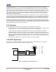
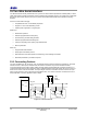
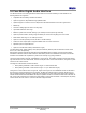
Table Of Contents
- 1 Introduction
- 2 Pin Configurations
- 3 CPU
- 4 Memory Organisation
- 5 System Clocks
- 6 Reset
- 7 Interrupt System
- 8 Wireless Transceiver
- 9 Digital Input/Output
- 10 Serial Peripheral Interface
- 11 Timers
- 12 Pulse Counters
- 13 Serial Communications
- 14 JTAG Debug Interface
- 15 Two-Wire Serial Interface
- 16 Four-Wire Digital Audio Interface
- 17 Random Number Generator
- 18 Sample FIFO
- 19 Intelligent Peripheral Interface
- 20 Analogue Peripherals
- 21 Power Management and Sleep Modes
- 22 Electrical Characteristics
- 22.1 Maximum Ratings
- 22.2 DC Electrical Characteristics
- 22.3 AC Characteristics
- 22.3.1 Reset and Voltage Brown-Out
- 22.3.2 SPI MasterTiming
- 22.3.3 Intelligent Peripheral (SPI Slave) Timing
- 22.3.4 Two-wire Serial Interface
- 22.3.5 Four-Wire Digital Audio Interface
- 22.3.6 Wakeup and Boot Load Timings
- 22.3.7 Bandgap Reference
- 22.3.8 Analogue to Digital Converters
- 22.3.9 Digital to Analogue Converters
- 22.3.10 Comparators
- 22.3.11 32kHz RC Oscillator
- 22.3.12 32kHz Crystal Oscillator
- 22.3.13 32MHz Crystal Oscillator
- 22.3.14 24MHz RC Oscillator
- 22.3.15 Temperature Sensor
- 22.3.16 Radio Transceiver
- Appendix A Mechanical and Ordering Information
- Appendix B Development Support

Jennic
46 JN-DS-JN5148-001 1v2 © Jennic 2009
Preliminary
15 Two-Wire Serial Interface
The JN5148 includes industry standard two-wire synchronous Serial Interface operates as a Master (MSIF) or Slave
(SSIF) that provides a simple and efficient method of data exchange between devices. The system uses a serial data
line (SIF_D) and a serial clock line (SIF_CLK) to perform bi-directional data transfers and includes the following
features:
Common to both master and slave:
• Compatible with both I
2
C and SMbus peripherals
• Support for 7 and 10-bit addressing modes
• Optional pulse suppression on signal inputs
Master only:
• Multi-master operation
• Software programmable clock frequency
• Clock stretching and wait state generation
• Software programmable acknowledge bit
• Interrupt or bit-polling driven byte-by-byte data-transfers
• Bus busy detection
Slave only:
• Programmable slave address
• Simple byte level transfer protocol
• Write data flow control with optional clock stretching or acknowledge mechanism
• Read data preloaded or provided as required
15.1 Connecting Devices
The clock and data lines, SIF_D and SIF_CLK, are alternate functions of DIO15 and DIO14 respectively. The serial
interface function of these pins is selected when the interface is enabled. They are both bi-directional lines,
connected internally to the positive supply voltage via weak (45kΩ) programmable pull-up resistors. However, it is
recommended that external 4.7kΩ pull-ups be used for reliable operation at high bus speeds, as shown in
Figure 31.
When the bus is free, both lines are HIGH. The output stages of devices connected to the bus must have an open-
drain or open-collector in order to perform the wired-AND function. The number of devices connected to the bus is
solely dependent on the bus capacitance limit of 400pF.
SIF_CL K
SIF_D
VDD
D1_OUT
D1_IN CLK1_IN
CLK1_OUT
D2_IN CLK2_IN
CLK2_OUT
DEVICE 1 DEVICE 2
R
P
R
P
Pu llup
Resistors
D2_OUT
JN5148
SIF
DIO14
DIO15
Figure 31: Connection Details