
User Manual
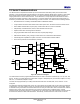
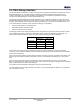
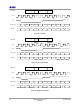
Table Of Contents
- 1 Introduction
- 2 Pin Configurations
- 3 CPU
- 4 Memory Organisation
- 5 System Clocks
- 6 Reset
- 7 Interrupt System
- 8 Wireless Transceiver
- 9 Digital Input/Output
- 10 Serial Peripheral Interface
- 11 Timers
- 12 Pulse Counters
- 13 Serial Communications
- 14 JTAG Debug Interface
- 15 Two-Wire Serial Interface
- 16 Four-Wire Digital Audio Interface
- 17 Random Number Generator
- 18 Sample FIFO
- 19 Intelligent Peripheral Interface
- 20 Analogue Peripherals
- 21 Power Management and Sleep Modes
- 22 Electrical Characteristics
- 22.1 Maximum Ratings
- 22.2 DC Electrical Characteristics
- 22.3 AC Characteristics
- 22.3.1 Reset and Voltage Brown-Out
- 22.3.2 SPI MasterTiming
- 22.3.3 Intelligent Peripheral (SPI Slave) Timing
- 22.3.4 Two-wire Serial Interface
- 22.3.5 Four-Wire Digital Audio Interface
- 22.3.6 Wakeup and Boot Load Timings
- 22.3.7 Bandgap Reference
- 22.3.8 Analogue to Digital Converters
- 22.3.9 Digital to Analogue Converters
- 22.3.10 Comparators
- 22.3.11 32kHz RC Oscillator
- 22.3.12 32kHz Crystal Oscillator
- 22.3.13 32MHz Crystal Oscillator
- 22.3.14 24MHz RC Oscillator
- 22.3.15 Temperature Sensor
- 22.3.16 Radio Transceiver
- Appendix A Mechanical and Ordering Information
- Appendix B Development Support

Jennic
© Jennic 2009 JN-DS-JN5148-001 1v2 45
Preliminary
14 JTAG Debug Interface
The JN5148 includes an IEEE1149.1 compliant JTAG port for the sole purpose of software code debug with Jennic's
Software Development Kit. The JTAG interface is disabled by default and is enabled under software control.
Therefore, debugging is only possible if enabled by the application. Once enabled, the application executes as
normal until the external debugger controller initiates debug activity.
The Debugger supports breakpoints and watchpoints based on four comparisons between any of program counter,
load/store effective address and load/store data. There is the ability to chain the comparisons together. There is also
the ability, under debugger control to perform the following commands: go, stop, reset, step over/into/out/next, run to
cursor and breakpoints. In addition, under control of the debugger, it is possible to:
• Read and write registers on the wishbone bus
• Read ROM and RAM, and write to RAM
• Read and write CPU internal registers
The Debugger interface is accessed, depending upon the configuration, through the pins used for UART0 or UART1.
This is enabled under software control and is dealt with in
JN-AN-1118 JN5148 Application Debugging [5]. The
following table details which DIO are used for the JTAG interface depending upon the configuration.
DIO Assignment Signal
UART0 pins UART1 pins
clock (TCK) 4 17
control (TMS) 5 18
data out (TDO) 6 19
data in (TDI) 7 16 or 20
Table 4 Hardware Debugger IO
If doze mode is active when debugging is started, the processor will be woken and then respond to debugger
commands. It is not possible to wake the device from sleep using the debug interface and debugging is not available
while the device is sleeping.
When using the debug interface, program execution is halted, and control of the CPU is handed to the debugger. The
watchdog, tick timer and the three timers described in section
11 are stalled while the debugger is in control of the
CPU.
When control is handed from the CPU to the debugger or back a small number of CPU clock cycles are taken
flushing or reloading the CPU pipeline. Because of this, when a program is halted by the debugger and then restarted
again, a small number of tick timer cycles will elapse.
It is possible to prevent all hardware debugging by blowing the relevant Efuse bit.
The JTAG interface does not support boundary scan testing. It is recommended that the JN5148 is not connected as
part of the board scan chain.