
User Manual
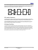
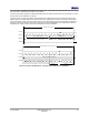
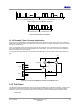
Table Of Contents
- 1 Introduction
- 2 Pin Configurations
- 3 CPU
- 4 Memory Organisation
- 5 System Clocks
- 6 Reset
- 7 Interrupt System
- 8 Wireless Transceiver
- 9 Digital Input/Output
- 10 Serial Peripheral Interface
- 11 Timers
- 12 Pulse Counters
- 13 Serial Communications
- 14 JTAG Debug Interface
- 15 Two-Wire Serial Interface
- 16 Four-Wire Digital Audio Interface
- 17 Random Number Generator
- 18 Sample FIFO
- 19 Intelligent Peripheral Interface
- 20 Analogue Peripherals
- 21 Power Management and Sleep Modes
- 22 Electrical Characteristics
- 22.1 Maximum Ratings
- 22.2 DC Electrical Characteristics
- 22.3 AC Characteristics
- 22.3.1 Reset and Voltage Brown-Out
- 22.3.2 SPI MasterTiming
- 22.3.3 Intelligent Peripheral (SPI Slave) Timing
- 22.3.4 Two-wire Serial Interface
- 22.3.5 Four-Wire Digital Audio Interface
- 22.3.6 Wakeup and Boot Load Timings
- 22.3.7 Bandgap Reference
- 22.3.8 Analogue to Digital Converters
- 22.3.9 Digital to Analogue Converters
- 22.3.10 Comparators
- 22.3.11 32kHz RC Oscillator
- 22.3.12 32kHz Crystal Oscillator
- 22.3.13 32MHz Crystal Oscillator
- 22.3.14 24MHz RC Oscillator
- 22.3.15 Temperature Sensor
- 22.3.16 Radio Transceiver
- Appendix A Mechanical and Ordering Information
- Appendix B Development Support

Jennic
© Jennic 2009 JN-DS-JN5148-001 1v2 35
Preliminary
sent from a slave, it should perform transmit using dummy data. An interrupt can be generated when the transaction
has completed or alternatively the interface can be polled.
If a slave device wishes to signal the JN5148 indicating that it has data to provide, it may be connected to one of the
DIO pins that can be enabled as an interrupt.
Figure 21 shows a complex SPI transfer, reading data from a FLASH device, that can be achieved using the SPI
master interface. The slave select line must stay low for many separate SPI accesses, and therefore manual slave
select mode must be used. The required slave select can then be asserted (active low) at the start of the transfer. A
sequence 8 and 32 bit transfers can be used to issue the command and address to the FLASH device and then to
read data back. Finally, the slave select can be deselected to end the transaction.
0
1234567
Instruction (0x03)
23 22 21 3 2 1 0
8 9 10 28 29 30 31
24-bit Address
MSB
Instruction Transaction
7 6 5 4 3 2 1 0
MSB
0
1234
57
8N-1
3 2 1 0
LSB
Read Data Bytes Transaction(s) 1-N
SPISEL
SPICLK
SPIMOSI
SPIMISO
SPISEL
SPICLK
SPIMOSI
SPIMISO
8910
7 6 5
MSB
Byte 1 Byte 2 Byte N
value unused by peripherals
6
Figure 21: Example SPI Waveforms – Reading from FLASH device using Mode 0