
User Manual
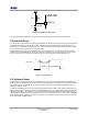

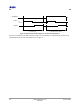

Table Of Contents
- 1 Introduction
- 2 Pin Configurations
- 3 CPU
- 4 Memory Organisation
- 5 System Clocks
- 6 Reset
- 7 Interrupt System
- 8 Wireless Transceiver
- 9 Digital Input/Output
- 10 Serial Peripheral Interface
- 11 Timers
- 12 Pulse Counters
- 13 Serial Communications
- 14 JTAG Debug Interface
- 15 Two-Wire Serial Interface
- 16 Four-Wire Digital Audio Interface
- 17 Random Number Generator
- 18 Sample FIFO
- 19 Intelligent Peripheral Interface
- 20 Analogue Peripherals
- 21 Power Management and Sleep Modes
- 22 Electrical Characteristics
- 22.1 Maximum Ratings
- 22.2 DC Electrical Characteristics
- 22.3 AC Characteristics
- 22.3.1 Reset and Voltage Brown-Out
- 22.3.2 SPI MasterTiming
- 22.3.3 Intelligent Peripheral (SPI Slave) Timing
- 22.3.4 Two-wire Serial Interface
- 22.3.5 Four-Wire Digital Audio Interface
- 22.3.6 Wakeup and Boot Load Timings
- 22.3.7 Bandgap Reference
- 22.3.8 Analogue to Digital Converters
- 22.3.9 Digital to Analogue Converters
- 22.3.10 Comparators
- 22.3.11 32kHz RC Oscillator
- 22.3.12 32kHz Crystal Oscillator
- 22.3.13 32MHz Crystal Oscillator
- 22.3.14 24MHz RC Oscillator
- 22.3.15 Temperature Sensor
- 22.3.16 Radio Transceiver
- Appendix A Mechanical and Ordering Information
- Appendix B Development Support

Jennic
28 JN-DS-JN5148-001 1v2 © Jennic 2009
Preliminary
TX Active
ADO (DIO[12])
1
st
TX-RX Cycle 2
nd
TX-RX Cycle (1
st
Retry)
RX Active
Figure 16 Antenna Diversity ADO Signal for TX with Acknowledgement
DIO13 can be configured to be ADE, the inverse of ADO. In this configuration, an antenna diversity scheme can be
implemented without the need for the inverter shown in
Figure 15.