
User Manual
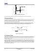

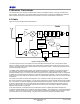

Table Of Contents
- 1 Introduction
- 2 Pin Configurations
- 3 CPU
- 4 Memory Organisation
- 5 System Clocks
- 6 Reset
- 7 Interrupt System
- 8 Wireless Transceiver
- 9 Digital Input/Output
- 10 Serial Peripheral Interface
- 11 Timers
- 12 Pulse Counters
- 13 Serial Communications
- 14 JTAG Debug Interface
- 15 Two-Wire Serial Interface
- 16 Four-Wire Digital Audio Interface
- 17 Random Number Generator
- 18 Sample FIFO
- 19 Intelligent Peripheral Interface
- 20 Analogue Peripherals
- 21 Power Management and Sleep Modes
- 22 Electrical Characteristics
- 22.1 Maximum Ratings
- 22.2 DC Electrical Characteristics
- 22.3 AC Characteristics
- 22.3.1 Reset and Voltage Brown-Out
- 22.3.2 SPI MasterTiming
- 22.3.3 Intelligent Peripheral (SPI Slave) Timing
- 22.3.4 Two-wire Serial Interface
- 22.3.5 Four-Wire Digital Audio Interface
- 22.3.6 Wakeup and Boot Load Timings
- 22.3.7 Bandgap Reference
- 22.3.8 Analogue to Digital Converters
- 22.3.9 Digital to Analogue Converters
- 22.3.10 Comparators
- 22.3.11 32kHz RC Oscillator
- 22.3.12 32kHz Crystal Oscillator
- 22.3.13 32MHz Crystal Oscillator
- 22.3.14 24MHz RC Oscillator
- 22.3.15 Temperature Sensor
- 22.3.16 Radio Transceiver
- Appendix A Mechanical and Ordering Information
- Appendix B Development Support

Jennic
26 JN-DS-JN5148-001 1v2 © Jennic 2009
Preliminary
8 Wireless Transceiver
The wireless transceiver comprises a 2.45GHz radio, modem, a baseband processor, a security coprocessor and
PHY controller. These blocks, with protocol software provided as a library, implement an IEEE802.15.4 standards-
based wireless transceiver that transmits and receives data over the air in the unlicensed 2.4GHz band.
8.1 Radio
Figure 14 shows the single ended radio architecture.
LNA
synth
PA
ADC
Reference
& Bias
Switch
Radio
Calibration
Lim1
Lim2
Lim3
Lim4
sigma
delta
D-Type
Figure 14: Radio Architecture
The radio comprises a low-IF receive path and a direct modulation transmit path, which converge at the TX/RX
switch. The switch connects to the external single ended matching network, which consists of two inductors and a
capacitor, this arrangement creates a 50Ω port and removes the need for a balun. A 50Ω single ended antenna can
be connected directly to this port.
The 32MHz crystal oscillator feeds a divider, which provides the frequency synthesiser with a reference frequency.
The synthesiser contains programmable feedback dividers, phase detector, charge pump and internal Voltage
Controlled Oscillator (VCO). The VCO has no external components, and includes calibration circuitry to compensate
for differences in internal component values due to process and temperature variations. The VCO is controlled by a
Phase Locked Loop (PLL) that has an internal loop filter. A programmable charge pump is also used to tune the loop
characteristic.
The receiver chain starts with the low noise amplifier / mixer combination whose outputs are passed to a lowpass
filter, which provides the channel definition. The signal is then passed to a series of amplifier blocks forming a limiting
strip. The signal is converted to a digital signal before being passed to the Modem. The gain control for the RX path
is derived in the automatic gain control (AGC) block within the Modem, which samples the signal level at various
points down the RX chain. To improve the performance and reduce current consumption, automatic calibration is
applied to various blocks in the RX path.
In the transmit direction, the digital stream from the Modem is passed to a digital sigma-delta modulator which
controls the feedback dividers in the synthesiser, (dual point modulation). The VCO frequency now tracks the applied
modulation. The 2.4 GHz signal from the VCO is then passed to the RF Power Amplifier (PA), whose power control
can be selected from one of three settings. The output of the PA drives the antenna via the RX/TX switch