
User Manual
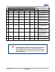

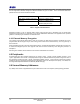
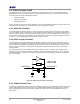
Table Of Contents
- 1 Introduction
- 2 Pin Configurations
- 3 CPU
- 4 Memory Organisation
- 5 System Clocks
- 6 Reset
- 7 Interrupt System
- 8 Wireless Transceiver
- 9 Digital Input/Output
- 10 Serial Peripheral Interface
- 11 Timers
- 12 Pulse Counters
- 13 Serial Communications
- 14 JTAG Debug Interface
- 15 Two-Wire Serial Interface
- 16 Four-Wire Digital Audio Interface
- 17 Random Number Generator
- 18 Sample FIFO
- 19 Intelligent Peripheral Interface
- 20 Analogue Peripherals
- 21 Power Management and Sleep Modes
- 22 Electrical Characteristics
- 22.1 Maximum Ratings
- 22.2 DC Electrical Characteristics
- 22.3 AC Characteristics
- 22.3.1 Reset and Voltage Brown-Out
- 22.3.2 SPI MasterTiming
- 22.3.3 Intelligent Peripheral (SPI Slave) Timing
- 22.3.4 Two-wire Serial Interface
- 22.3.5 Four-Wire Digital Audio Interface
- 22.3.6 Wakeup and Boot Load Timings
- 22.3.7 Bandgap Reference
- 22.3.8 Analogue to Digital Converters
- 22.3.9 Digital to Analogue Converters
- 22.3.10 Comparators
- 22.3.11 32kHz RC Oscillator
- 22.3.12 32kHz Crystal Oscillator
- 22.3.13 32MHz Crystal Oscillator
- 22.3.14 24MHz RC Oscillator
- 22.3.15 Temperature Sensor
- 22.3.16 Radio Transceiver
- Appendix A Mechanical and Ordering Information
- Appendix B Development Support

Jennic
18 JN-DS-JN5148-001 1v2 © Jennic 2009
Preliminary
At reset, the contents of this memory are copied into RAM by the software boot loader. The Flash memory devices
that are supported as standard through the JN5148 bootloader are given in Table 1. Jennic recommends that where
possible one of these devices should be selected.
Manufacturer Device Number
SST (Silicon Storage Technology) 25VF010A (1Mbyte device)
Numonyx M25P10-A (1Mbyte device),
M25P40 (4Mbyte device)
Table 1: Supported Flash Memories
Applications wishing to use an alternate Flash memory device should refer to application note [3] JN-AN-1038
Programming Flash devices not supported by the JN51xx ROM-based bootloader. This application note provides
guidance on developing an interface to an alternate device.
4.4.1 External Memory Encryption
The contents of the external serial memory may be encrypted. The AES security processor combined with a user
programmable 128-bit encryption key is used to encrypt the contents of the external memory. The encryption key is
stored in eFuse.
When bootloading program code from external serial memory, the JN5148 automatically accesses the encryption key
to execute the decryption process. User program code does not need to handle any of the decryption process; it is
transparent.
With encryption enabled, the time taken to boot code from external flash is increased.
4.5 Peripherals
All peripherals have their registers mapped into the memory space. Access to these registers requires 3 clock
cycles. Applications have access to the peripherals through the software libraries that present a high-level view of
the peripheral’s functions through a series of dedicated software routines. These routines provide both a tested
method for using the peripherals and allow bug-free application code to be developed more rapidly. For details, see
the Integrated Peripherals API Reference Manual (JN-RM-2001).[6]
4.6 Unused Memory Addresses
Any attempt to access an unpopulated memory area will result in a bus error exception (interrupt) being generated.