
User Manual

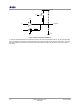
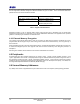
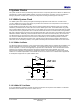
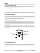
Table Of Contents
- 1 Introduction
- 2 Pin Configurations
- 3 CPU
- 4 Memory Organisation
- 5 System Clocks
- 6 Reset
- 7 Interrupt System
- 8 Wireless Transceiver
- 9 Digital Input/Output
- 10 Serial Peripheral Interface
- 11 Timers
- 12 Pulse Counters
- 13 Serial Communications
- 14 JTAG Debug Interface
- 15 Two-Wire Serial Interface
- 16 Four-Wire Digital Audio Interface
- 17 Random Number Generator
- 18 Sample FIFO
- 19 Intelligent Peripheral Interface
- 20 Analogue Peripherals
- 21 Power Management and Sleep Modes
- 22 Electrical Characteristics
- 22.1 Maximum Ratings
- 22.2 DC Electrical Characteristics
- 22.3 AC Characteristics
- 22.3.1 Reset and Voltage Brown-Out
- 22.3.2 SPI MasterTiming
- 22.3.3 Intelligent Peripheral (SPI Slave) Timing
- 22.3.4 Two-wire Serial Interface
- 22.3.5 Four-Wire Digital Audio Interface
- 22.3.6 Wakeup and Boot Load Timings
- 22.3.7 Bandgap Reference
- 22.3.8 Analogue to Digital Converters
- 22.3.9 Digital to Analogue Converters
- 22.3.10 Comparators
- 22.3.11 32kHz RC Oscillator
- 22.3.12 32kHz Crystal Oscillator
- 22.3.13 32MHz Crystal Oscillator
- 22.3.14 24MHz RC Oscillator
- 22.3.15 Temperature Sensor
- 22.3.16 Radio Transceiver
- Appendix A Mechanical and Ordering Information
- Appendix B Development Support

Jennic
© Jennic 2009 JN-DS-JN5148-001 1v2 17
Preliminary
4.2 RAM
The JN5148 contains 128kBytes of high speed RAM. It can be used for both code and data storage and is accessed
by the CPU in a single clock cycle. At reset, a boot loader controls the loading of segments of code and data from an
external memory connected to the SPI port, into RAM. Software can control the power supply to the RAM allowing
the contents to be maintained during a sleep period when other parts of the device are un-powered. Typical RAM
contents are shown in Figure 7.
MAC Data
Interrupt Vector Table
Application
CPU Stack
(Grows Down)
0x04000000
0x04020000
MAC Address
Figure 7: Typical RAM Contents
4.3 OTP eFuse Memory
The JN5148 contains a total of 32bytes of eFuse memory; this is a One Time Programmable (OTP) memory that is
used to support on chip 64-bit MAC ID and a 128-bit AES security key. A limited number of bits are available for
customer use for storage of configuration information; configuration of these is made through use of software APIs.
For full details on how to program and use the eFuse memory, please refer to application note
JN-AN-1062 Using
OTP efuse Memory
[2]
Alternatively, Jennic can provide an eFuse programming service for customers that wish to use the eFuse but do not
wish to undertake this for themselves. For further details of this service, please contact your local Jennic sales office.
4.4 External Memory
An external memory with an SPI interface may be used to provide storage for program code and data for the device
when external power is removed. The memory is connected to the SPI interface using select line SPISEL0; this
select line is dedicated to the external memory interface and is not available for use with other external devices. See
Figure 8 for connection details.
JN5148
Serial
Me mor y
SPISEL0
SPIMISO
SPIMOSI
SPICLK
SS
SDO
SDI
CLK
Figure 8: Connecting External Serial Memory