
User Manual
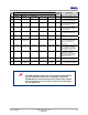

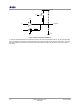
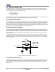
Table Of Contents
- 1 Introduction
- 2 Pin Configurations
- 3 CPU
- 4 Memory Organisation
- 5 System Clocks
- 6 Reset
- 7 Interrupt System
- 8 Wireless Transceiver
- 9 Digital Input/Output
- 10 Serial Peripheral Interface
- 11 Timers
- 12 Pulse Counters
- 13 Serial Communications
- 14 JTAG Debug Interface
- 15 Two-Wire Serial Interface
- 16 Four-Wire Digital Audio Interface
- 17 Random Number Generator
- 18 Sample FIFO
- 19 Intelligent Peripheral Interface
- 20 Analogue Peripherals
- 21 Power Management and Sleep Modes
- 22 Electrical Characteristics
- 22.1 Maximum Ratings
- 22.2 DC Electrical Characteristics
- 22.3 AC Characteristics
- 22.3.1 Reset and Voltage Brown-Out
- 22.3.2 SPI MasterTiming
- 22.3.3 Intelligent Peripheral (SPI Slave) Timing
- 22.3.4 Two-wire Serial Interface
- 22.3.5 Four-Wire Digital Audio Interface
- 22.3.6 Wakeup and Boot Load Timings
- 22.3.7 Bandgap Reference
- 22.3.8 Analogue to Digital Converters
- 22.3.9 Digital to Analogue Converters
- 22.3.10 Comparators
- 22.3.11 32kHz RC Oscillator
- 22.3.12 32kHz Crystal Oscillator
- 22.3.13 32MHz Crystal Oscillator
- 22.3.14 24MHz RC Oscillator
- 22.3.15 Temperature Sensor
- 22.3.16 Radio Transceiver
- Appendix A Mechanical and Ordering Information
- Appendix B Development Support

Jennic
© Jennic 2009 JN-DS-JN5148-001 1v2 15
Preliminary
3 CPU
The CPU of the JN5148 is a 32-bit load and store RISC processor. It has been architected for three key
requirements:
• Low power consumption for battery powered applications
• High performance to implement a wireless protocol at the same time as complex applications
• Efficient coding of high-level languages such as C provided with the Jennic Software Developers Kit
It features a linear 32-bit logical address space with unified memory architecture, accessing both code and data in the
same address space. Registers for peripheral units, such as the timers, UARTs and the baseband processor are
also mapped into this space.
The CPU has access to a block of 15 32-bit General-Purpose (GP) registers together with a small number of special
purpose registers which are used to store processor state and control interrupt handling. The contents of any GP
register can be loaded from or stored to memory, while arithmetic and logical operations, shift and rotate operations,
and signed and unsigned comparisons can be performed either between two registers and stored in a third, or
between registers and a constant carried in the instruction. Operations between general or special-purpose registers
execute in one cycle while those that access memory require a further cycle to allow the memory to respond.
The instruction set manipulates 8, 16 and 32-bit data; this means that programs can use objects of these sizes very
efficiently. Manipulation of 32-bit quantities is particularly useful for protocols and high-end applications allowing
algorithms to be implemented in fewer instructions than on smaller word-size processors, and to execute in fewer
clock cycles. In addition, the CPU supports hardware Multiply that can be used to efficiently implement algorithms
needed by Digital Signal Processing applications.
The instruction set is designed for the efficient implementation of high-level languages such as C. Access to fields in
complex data structures is very efficient due to the provision of several addressing modes, together with the ability to
be able to use any of the GP registers to contain the address of objects. Subroutine parameter passing is also made
more efficient by using GP registers rather than pushing objects onto the stack. The recommended programming
method for the JN5148 is by using C, which is supported by a software developer kit comprising a C compiler, linker
and debugger.
The CPU architecture also contains features that make the processor suitable for embedded, real-time applications.
In some applications, it may be necessary to use a real-time operating system to allow multiple tasks to run on the
processor. To provide protection for device-wide resources being altered by one task and affecting another, the
processor can run in either supervisor or user mode, the former allowing access to all processor registers, while the
latter only allows the GP registers to be manipulated. Supervisor mode is entered on reset or interrupt; tasks starting
up would normally run in user mode in a RTOS environment.
Embedded applications require efficient handling of external hardware events. Exception processing (including reset
and interrupt handling) is enhanced by the inclusion of a number of special-purpose registers into which the PC and
status register contents are copied as part of the operation of the exception hardware. This means that the essential
registers for exception handling are stored in one cycle, rather than the slower method of pushing them onto the
processor stack. The PC is also loaded with the vector address for the exception that occurred, allowing the handler
to start executing in the next cycle.
To improve power consumption a number of power-saving modes are implemented in the JN5148, described more
fully in section
21 - Power Management and Sleep Modes. One of these modes is the CPU doze mode; under
software control, the processor can be shut down and on an interrupt it will wake up to service the request.
Additionally, it is possible under software control, to set the speed of the CPU to 4, 8, 16 or 32MHz. This feature can
be used to trade-off processing power against current consumption.