
User Manual

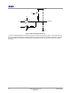
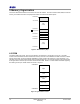
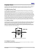
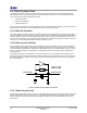
Table Of Contents
- 1 Introduction
- 2 Pin Configurations
- 3 CPU
- 4 Memory Organisation
- 5 System Clocks
- 6 Reset
- 7 Interrupt System
- 8 Wireless Transceiver
- 9 Digital Input/Output
- 10 Serial Peripheral Interface
- 11 Timers
- 12 Pulse Counters
- 13 Serial Communications
- 14 JTAG Debug Interface
- 15 Two-Wire Serial Interface
- 16 Four-Wire Digital Audio Interface
- 17 Random Number Generator
- 18 Sample FIFO
- 19 Intelligent Peripheral Interface
- 20 Analogue Peripherals
- 21 Power Management and Sleep Modes
- 22 Electrical Characteristics
- 22.1 Maximum Ratings
- 22.2 DC Electrical Characteristics
- 22.3 AC Characteristics
- 22.3.1 Reset and Voltage Brown-Out
- 22.3.2 SPI MasterTiming
- 22.3.3 Intelligent Peripheral (SPI Slave) Timing
- 22.3.4 Two-wire Serial Interface
- 22.3.5 Four-Wire Digital Audio Interface
- 22.3.6 Wakeup and Boot Load Timings
- 22.3.7 Bandgap Reference
- 22.3.8 Analogue to Digital Converters
- 22.3.9 Digital to Analogue Converters
- 22.3.10 Comparators
- 22.3.11 32kHz RC Oscillator
- 22.3.12 32kHz Crystal Oscillator
- 22.3.13 32MHz Crystal Oscillator
- 22.3.14 24MHz RC Oscillator
- 22.3.15 Temperature Sensor
- 22.3.16 Radio Transceiver
- Appendix A Mechanical and Ordering Information
- Appendix B Development Support

Jennic
12 JN-DS-JN5148-001 1v2 © Jennic 2009
Preliminary
2.2 Pin Descriptions
2.2.1 Power Supplies
The device is powered from the VDD1 and VDD2 pins, each being decoupled with a 100nF ceramic capacitor. VDD1
is the power supply to the analogue circuitry; it should be decoupled to ground. VDD2 is the power supply for the
digital circuitry; and should also be decoupled to ground. A 10uF tantalum capacitor is required. Decoupling pins for
the internal 1.8V regulators are provided which require a 100nF capacitor located as close to the device as practical.
VB_VCO, VB_RF, VB_A and VB_SYNTH should be decoupled with an additional 47pF capacitor, while VB_RAM
and VB_DIG require only 100nF. VB_RF and VB_RF2 should be connected together as close to the device as
practical, and only require one 100nF capacitor and one 47pF capacitor. Refer to
B.4.1 for schematic diagram.
VSSA, VSSS, VSS1, VSS2, VSS3 are the ground pins.
2.2.2 Reset
RESETN is a bi-directional active low reset pin that is connected to a 40kΩ internal pull-up resistor. It may be pulled
low by an external circuit, or can be driven low by the JN5148 if an internal reset is generated. Typically, it will be
used to provide a system reset signal. Refer to section 6.2, External Reset, for more details.
2.2.3 32MHz Oscillator
A crystal is connected between XTALIN and XTALOUT to form the reference oscillator, which drives the system
clock. A capacitor to analogue ground is required on each of these pins. Refer to section
5.1 16MHz System Clock
for more details. The 32MHz reference frequency is divided down to 16MHz and this is used as the system clock
throughout the device.
2.2.4 Radio
The radio is a single ended design, requiring a capacitor and just two inductors to match to 50Ω microstrip line to the
RF_IN pin.
An external resistor (43kΩ) is required between IBIAS and analogue ground to set various bias currents and
references within the radio.