
User Manual
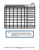

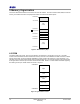
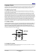
Table Of Contents
- 1 Introduction
- 2 Pin Configurations
- 3 CPU
- 4 Memory Organisation
- 5 System Clocks
- 6 Reset
- 7 Interrupt System
- 8 Wireless Transceiver
- 9 Digital Input/Output
- 10 Serial Peripheral Interface
- 11 Timers
- 12 Pulse Counters
- 13 Serial Communications
- 14 JTAG Debug Interface
- 15 Two-Wire Serial Interface
- 16 Four-Wire Digital Audio Interface
- 17 Random Number Generator
- 18 Sample FIFO
- 19 Intelligent Peripheral Interface
- 20 Analogue Peripherals
- 21 Power Management and Sleep Modes
- 22 Electrical Characteristics
- 22.1 Maximum Ratings
- 22.2 DC Electrical Characteristics
- 22.3 AC Characteristics
- 22.3.1 Reset and Voltage Brown-Out
- 22.3.2 SPI MasterTiming
- 22.3.3 Intelligent Peripheral (SPI Slave) Timing
- 22.3.4 Two-wire Serial Interface
- 22.3.5 Four-Wire Digital Audio Interface
- 22.3.6 Wakeup and Boot Load Timings
- 22.3.7 Bandgap Reference
- 22.3.8 Analogue to Digital Converters
- 22.3.9 Digital to Analogue Converters
- 22.3.10 Comparators
- 22.3.11 32kHz RC Oscillator
- 22.3.12 32kHz Crystal Oscillator
- 22.3.13 32MHz Crystal Oscillator
- 22.3.14 24MHz RC Oscillator
- 22.3.15 Temperature Sensor
- 22.3.16 Radio Transceiver
- Appendix A Mechanical and Ordering Information
- Appendix B Development Support

Jennic
© Jennic 2009 JN-DS-JN5148-001 1v2 11
Preliminary
Digital Peripheral I/O Pin
No
Primary Alternate Functions
Signal
Type
Description
51 DIO10 TIM0OUT 32KXTALOUT CMOS DIO10, Timer0 PWM Output or
32K External Crystal Output
52 DIO11 TIM1CK_GT TIM2OUT CMOS DIO11, Timer1 Clock/Gate
Input or Timer2 PWM Output
53 DIO12 TIM1CAP ADO DAI_WS CMOS DIO12, Timer1 Capture Input,
Antenna Diversity or Digital
Audio Word Select
54 DIO13 TIM1OUT ADE DAI_SDIN CMOS DIO13, Timer1 PWM Output,
Antenna Diversity or Digital
Audio Data Input
55 DIO14 SIF_CLK IP_CLK CMOS DIO14, Serial Interface Clock
or Intelligent Peripheral Clock
Input
56 DIO15 SIF_D IP_DO CMOS DIO15, Serial Interface Data or
Intelligent Peripheral Data Out
1 DIO16 RXD1
(optional)
IP_DI JTAG_TDI
(optional)
CMOS DIO16, UART 1 Receive Data
Input or Intelligent Peripheral
Data In or JTAG data In
(optional)
2 DIO17 CTS1 IP_SEL DAI_SCK JTAG_TCK CMOS DIO17, UART 1 Clear To Send
Input, Intelligent Peripheral
Device Select Input or Digital
Audio Clock or JTAG CLK
4 DIO18 RTS1 IP_INT DAI_SDOUT JTAG_TMS CMOS DIO18, UART 1 Request To
Send Output, Intelligent
Peripheral Interrupt Output or
Digital Audio Data Output or
JTAG Mode Select
5 DIO19 TXD1 JTAG_TDO CMOS DIO19 or UART 1 Transmit
Data Output or JTAG Data Out
31 DIO 20 RXD1
(default)
JTAG_TDI
(default)
CMOS DIO 20, UART 1 Receive Data
Input or JTAG data In (default)
The PCB schematic and layout rules detailed in Appendix B.4
must be followed. Failure to do so will likely result in the
JN5148 failing to meet the performance specification detailed
herein and worst case may result in device not functioning in
the end application.