
Data Sheet

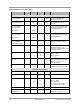
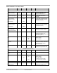


© NXP Laboratories UK 2012 JN-DS-JN5142 1v0 77
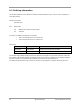
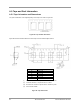
The PCB schematic and layout rules detailed in Appendix B.4 must
be followed. Failure to do so will likely result in the JN5142 failing
to meet the performance specification detailed herein and worst
case may result in device not functioning in the end application.