
Data Sheet


76 JN-DS-JN5142 1v0 © NXP Laboratories UK 2012
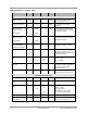
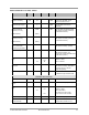
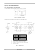
A.2 Footprint information
Information for reflow soldering. All dimensions are given in the table underneath.
Figure 46: PCB Decal
P
Ax
Ay
Bx
By
C
D
SLx
Sly
SPx tot
Spy tot
SPx
Spy
Gx
Gy
Hx
Hy
0.500
7.000
7.000
5.200
5.200
0.900
0.290
4.100
4.100
2.400
2.400
0.600
0.600
6.300
6.300
7.250
7.250
Table 12: Footprint Dimensions