
Data Sheet


66 JN-DS-JN5142 1v0 © NXP Laboratories UK 2012
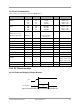
19.3.7 Comparator
VDD = 2.0 to 3.6V -40 to +125ºC, italic +85 ºC Bold +125 ºC
Parameter
Min
Typ
Max
Unit
Notes
Analogue response time
(normal)
85
125,130
ns
+/- 250mV overdrive
10pF load
Total response time
(normal) including delay to
Interrupt controller
105
+ 125,130
ns
Digital delay can be
up to a max. of two
16MHz clock periods
Analogue response time
(low power)
2.4
2.8
µs
+/- 250mV overdrive
No digital delay
Hysteresis
4
12
28
10
20
40
16, 17
26, 29
50, 55
mV
Programmable in 3
steps and zero
Vref (Internal)
See Section 19.3.5
V
Common Mode input range
0
Vdd
V
Current (normal mode)
54
73
102, 110
µA
Current (low power mode)
0.8
1.1, 1.2
µA
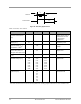
19.3.8 32kHz RC Oscillator
VDD = 2.0 to 3.6V, -40 to +125 ºC, italic +85 ºC Bold +125 ºC
Parameter
Min
Typ
Max
Unit
Notes
Current consumption of cell
and counter logic
680
600
500
830, 930
750, 850
650, 710
nA
3.6V
3.0V
2.0V
32kHz clock native
accuracy
-30%
32kHz
+30%
Typical is at 3.0V 25C
Calibrated 32kHz accuracy
±250
ppm
For a 1 second sleep
period calibrating over
20 x 32kHz clock
periods
Variation with temperature
-0.010
%/°C
Variation with VDD2
-1.8
%/V