
Data Sheet


© NXP Laboratories UK 2012 JN-DS-JN5142 1v0 55
17.1.1 Operation
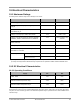
The input range of the ADC can be set between 0V to either the reference voltage or twice the reference voltage.
The reference can be either taken from the internal voltage reference or from the external voltage applied to the
VREF pin. For example, an external reference of 1.2V supplied to VREF may be used to set the ADC range between
0V and 2.4V.
VREF
Gain Setting
Maximum Input Range
Supply Voltage Range (VDD)
1.2V
1.6V
1.2V
1.6V
0
0
1
1
1.2V
1.6V
2.4V
3.2V
2.2V - 3.6V
2.2V - 3.6V
2.6V - 3.6V
3.4V - 3.6V
Table 10: ADC Maximum Input Range
The input clock to the ADC is 16MHz and can be divided down to 2MHz, 1MHz, 500kHz and 250kHz. During an ADC
conversion the selected input channel is sampled for a fixed period and then held. This sampling period is defined as
a number of ADC clock periods and can be programmed to 2, 4, 6 or 8. The conversion rate is ((3 x Sample period)
+ 10) clock periods. For example for 500kHz conversion with sample period of 2 will be (3 x 2) + 10 = 16 clock
periods, 32µsecs or 31.25kHz. The ADC can be operated in either a single conversion mode or alternatively a new
conversion can be started as soon as the previous one has completed, to give continuous conversions.
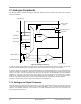
If the source resistance of the input voltage is 1kΩ or less, then the default sampling time of 2 clocks should be used.
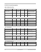
The input to the ADC can be modelled as a resistor of 5kΩ(typ) and 10kΩ (max) to represent the on-resistance of the
switches and the sampling capacitor 8pF. The sampling time required can then be calculated, by adding the sensor
source resistance to the switch resistance, multiplying by the capacitance giving a time constant. Assuming normal
exponential RC charging, the number of time constants required to give an acceptable error can be calculated, 6 time
constants gives an error of 0.25%, so for 8-bit accuracy 7 time constants should be the target. For a source with zero
resistance, 7 time constants is 560 nsecs, hence the smallest sampling window of 2 clock periods can be used.
ADC
pin
5 K
8 pF
Sample
Switch
ADC
front
end
Figure 39: ADC Input Equivalent Circuit
The ADC sampling period, input range and mode (single shot or continuous) are controlled through software.
When the ADC conversion is complete, an interrupt is generated. Alternatively the conversion status can be polled.
When operating in continuous mode, it is recommended that the interrupt is used to signal the end of a conversion,
since conversion times may range from 8 to 136 secs. Polling over this period would be wasteful of processor
bandwidth.
To facilitate averaging of the ADC values, which is a common practice in microcontrollers, a dedicated accumulator
has been added, the user can define the accumulation to occur over 2,4,8 or 16 samples. The end of conversion
interrupt can be modified to occur at the end of the chosen accumulation period, alternatively polling can still be used.
Software can then be used to apply the appropriate rounding and shifting to generate the average value, as well as
setting up the accumulation function.
For detailed electrical specifications, see Section 19.3.6.