
Data Sheet


4 JN-DS-JN5142 1v0 © NXP Laboratories UK 2012
18.2 Active Processing Mode 57
18.2.1 CPU Doze 57
18.3 Sleep Mode 57
18.3.1 Wakeup Timer Event 58
18.3.2 DIO Event 58
18.3.3 Comparator Event 58
18.3.4 Pulse Counter 58
18.4 Deep Sleep Mode 58
19 Electrical Characteristics 59
19.1 Maximum Ratings 59
19.2 DC Electrical Characteristics 59
19.2.1 Operating Conditions 59
19.2.2 DC Current Consumption 60
19.2.3 I/O Characteristics 61
19.3 AC Characteristics 61
19.3.1 Reset and Supply Voltage Monitor 61
19.3.2 SPI Master Timing 63
19.3.3 Two-wire Serial Interface 64
19.3.4 Wakeup and Boot Load Timings 64
19.3.5 Bandgap Reference 65
19.3.6 Analogue to Digital Converters 65
19.3.7 Comparator 66
19.3.8 32kHz RC Oscillator 66
19.3.9 32kHz Crystal Oscillator 67
19.3.10 32MHz Crystal Oscillator 67
19.3.11 High-Speed RC Oscillator 68
19.3.12 Temperature Sensor 68
19.3.13 Radio Transceiver 69
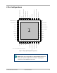
Appendix A Mechanical and Ordering Information 75
A.1 SOT618-1 HVQFN40 40-pin QFN Package Drawing 75
A.2 Footprint information 76
A.3 Ordering Information 78
A.4 Device Package Marking 79
A.5 Tape and Reel Information 80
A.5.1 Tape Orientation and Dimensions 80
A.5.2 Reel Information: 180mm Reel 81
A.5.3 Reel Information: 330mm Reel 82
A.5.4 Dry Pack Requirement for Moisture Sensitive Material 82
Appendix B Development Support 83
B.1 Crystal Oscillators 83
B.1.1 Crystal Equivalent Circuit 83
B.1.2 Crystal Load Capacitance 83
B.1.3 Crystal ESR and Required Transconductance 84
B.2 32MHz Oscillator 85
B.3 32kHz Oscillator 87
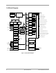
B.4 JN5142 Module Reference Designs 89
B.4.1 Schematic Diagram 89
B.4.2 PCB Design and Reflow Profile 92
B.4.3 Moisture Sensitivity Level (MSL) 92