
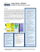
Data Sheet


2 JN-DS-JN5142 1v0 © NXP Laboratories UK 2012
Contents
1 Introduction 6
1.1 Wireless Transceiver 6
1.2 RISC CPU and Memory 6
1.3 Peripherals 7
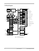
1.4 Block Diagram 8
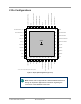
2 Pin Configurations 9
2.1 Pin Assignment 10
2.2 Pin Descriptions 12
2.2.1 Power Supplies 12
2.2.2 Reset 12
2.2.3 32MHz Oscillator 12
2.2.4 Radio 12
2.2.5 Analogue Peripherals 13
2.2.6 Digital Input/Output 13
3 CPU 15
4 Memory Organisation 16
4.1 ROM 16
4.2 RAM 17
4.3 OTP eFuse Memory 17
4.4 External Memory 17
4.4.1 External Memory Encryption 18
4.5 Peripherals 18
4.6 Unused Memory Addresses 18
5 System Clocks 19
5.1 16MHz System Clock 19
5.1.1 32MHz Oscillator 19
5.1.2 High-Speed RC Oscillator 20
5.2 32kHz System Clock 20
5.2.1 32kHz RC Oscillator 20
5.2.2 32kHz Crystal Oscillator 20
5.2.3 32kHz External Clock 21
6 Reset 22
6.1 Internal Brown-out Reset 22
6.2 External Reset 23
6.3 Software Reset 23
6.4 Supply Voltage Monitor (SVM) 23
6.5 Watchdog Timer 24
7 Interrupt System 25
7.1 System Calls 25
7.2 Processor Exceptions 25
7.2.1 Bus Error 25
7.2.2 Alignment 25
7.2.3 Illegal Instruction 25
7.2.4 Stack Overflow 25
7.3 Hardware Interrupts 26