USER GUIDE Tegra™ 200 Series Developer Board Advance Information – Subject to Change NVIDIA CONFIDENTIAL January 2010 | DG-04927-001_v01
Document Change History 2 Version Date Description v01 JAN 22, 2010 Initial Release Advance Information – Subject to Change NVIDIA CONFIDENTIAL DG-04927-001_v01
Tegra 200 Series Developer Board User Guide Table of Contents 1.0 INTRODUCTION ....................................................................................................................................................................5 2.0 DEVELOPER BOARD OVERVIEW ........................................................................................................................................6 2.1 Feature List ..................................................................................
Tegra 200 Series Developer Board User Guide 4.6 Display..............................................................................................................................................................................27 4.6.1 LCD Displays ............................................................................................................................................................................... 27 4.6.2 HDMI ......................................................................
Tegra 200 Series Developer Board User Guide 1.0 INTRODUCTION The Smartbook Development System is an example of a development platform built around the Tegra™ 200 Series Developer Board. This example provides a starting point for continued development; it outlines a fairly typical Smartbook configuration based on the NVIDIA® Tegra™ 250 Computer-on-a-Chip.
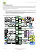
Tegra 200 Series Developer Board User Guide 2.0 DEVELOPER BOARD OVERVIEW 2.1 Feature List Applications Processor NVIDIA Tegra 250, 23x23mm ,0.
Tegra 200 Series Developer Board User Guide Figure 2.
Tegra 200 Series Developer Board User Guide 2.2 NVIDIA® Tegra™ 250 The NVIDIA Tegra 250 computer-on-a-chip is suited for handheld and mobile applications. It’s primary purpose is to control all system peripherals and provide computing power.
Tegra 200 Series Developer Board User Guide 2.5 LCD Interface The Smartbook Development System routes an 18-bit parallel RGB interface from the Tegra 250 to a Texas Instruments SN75LVDS83B LVDS Transmitter which goes to an LVDS panel connector (J7). The connector is a Foxconn GS13307-112307F. The controls available for the panel and backlight include: Panel power provided by main 3.
Tegra 200 Series Developer Board User Guide of the USB ports are brought to standard Type A connectors (J6 – Dual host port connector and J25 – Single host port). The forth USB is routed to PCIe Mini-Card #1 (J28). 2.9 Storage There are two SD/MMC sockets on the Tegra 200 Series Developer Board.
Tegra 200 Series Developer Board User Guide 2.12 User Interface Attach your USB keyboard and mouse to any of the available USB Type-A Host ports (J6, J25). 2.13 Miscellaneous Temperature Sensor On Semiconductor Model ADT7461AARMZ_RL7 0.25°C resolution/1°C accuracy (remote channel used) Interfaces to PWR_I2C Programmable over/under temperature limits Debug Options The Tegra 200 Series Developer Board provides development/debugging interfaces including JTAG, UART and Ethernet.
Tegra 200 Series Developer Board User Guide 3.0 SATELLITE BOARD HEADERS Two dual row 50-pin expansion headers enable the ability to connect a satellite board to the Tegra 200 Series Developer Board and are used to extend developer board functionality. Figure 4.
Tegra 200 Series Developer Board User Guide 3.1 Satellite Board Headers All the interface connections between a satellite board and the Tegra 200 Series Developer Board are through two sets of Samtec FTS series 50-pin Micro Strips connectors. Table 2.
Tegra 200 Series Developer Board User Guide 3.2 I2C Map The I2C interface can be used to connect a touch screen, touch pad and other devices. There are two options for the Touch devices. I2C versions of these devices (recommended) interface to the Tegra 250, while PS/2 versions connect to the EC controller. Table 3. Tegra 200 Series Developer Board I2C Map Domain Contrlr Pins Volt. Device ID / I2C Addr Location Main Board VDDIO_VI I2C3 CAM_I2C_SCL/SDA 3.
Tegra 200 Series Developer Board User Guide 4.0 CONNECTION EXAMPLES 4.1 Power Figure 6.
Tegra 200 Series Developer Board User Guide 4.1.1 Major Components 4.1.1.1 PMU The Tegra 200 Series Developer Board includes a multi-channel power management unit for embedded processors (TI TPS658621). Feature List Host Interface I2C Control I/F Core/CPU power request signals 32.768KHz Clock Reset input Reset output RTC LDO 1.0V-1.
Tegra 200 Series Developer Board User Guide 4.1.2 Power Supplies The Tegra 250 has 29 power rails (3 cores, 14 analog and 12 digital I/O). Depending on system design, many of the rails can share a power supply, and some are not needed for all designs. The example shown in Table 4 is based on the Smartbook Development System design and should be representative of these types of designs. This table mainly lists the supplies required by the Tegra 250.
Tegra 200 Series Developer Board User Guide 4.1.3 Power Sequencing The Power solution, including the PMU and any external supplies/logic, must be able to meet the Tegra 250 power sequence requirements. These requirements are detailed in the Tegra 200 Series datasheet (Electrical, Mechanical and Thermal Specifications). Figure 7 shows the sequence used for the Smartbook Development System. Figure 7. Power-up Sequence Example VBAT (10.2-12.6V, 15V) VDD_5V0 (5V, DC/DC TPS51220A) VDD_3V3_SBY (3.
Tegra 200 Series Developer Board User Guide 4.1.4 Bypass Capacitor Recommendations Table 5 lists the basic recommendations for bypass capacitors near the Tegra 250. In general, one 0.1uf per power pin (or group for cores) is desirable. These should be placed as close as possible to the respective power pins. In addition, for the higher power/higher frequency I/O rails one or more 4.7uf bulk capacitor is recommended and should be placed in the general area of the power and interface pins.
Tegra 200 Series Developer Board User Guide 4.2 Clocks The Tegra 250 has a large number of internal functional blocks supporting a broad range of interfaces. Each of these has its own clocking requirements. The RTC (Real Time Clock) and PMC (Power Management Controller) require a 32.768KHz clock, to be provided externally. In addition, a higher frequency reference clock (OSC) is required.
Tegra 200 Series Developer Board User Guide Figure 9.
Tegra 200 Series Developer Board User Guide 4.3 DRAM Memory Configurations Tegra 250 supports standard DDR2 SDRAM. Up to 1GB total memory, two chip selects and two Clock Enables are supported. A full 8-device configurations using x8 DDR2 devices is shown. A 4 device configuration is possible and is a subset of the 8 device configuration. Only Rank 0 would be used in this case. 4.3.
Tegra 200 Series Developer Board User Guide Table 7.
Tegra 200 Series Developer Board User Guide 4.4 NAND The Tegra 250 GMI interface supports a broad range of devices including a variety of NAND devices and configurations. Works with SLC and MLC devices Supports up to 8 devices with up to 8 chip selects Figure 11. Single 8-bit NAND Connection Example 4.5 USB The Tegra 250 has three available USB controllers. Controllers #1 and #3 come out on the USB PHYs on the USB1 and USB3 pins.
Tegra 200 Series Developer Board User Guide 4.5.1 Force Recovery The Tegra 250 requires USB1 to be available as a Device for Force Recovery mode which is used to download new firmware. This is shown in Figure 12 where a USB Mini B connector is available to connect to a Host system. Force Recovery mode is entered by keeping the FORCE_RECOVERY pin low when the system is first powered up (until SYS_RESET_N goes high. This is accomplished by pressing the momentary push button shown during power-on.
Tegra 200 Series Developer Board User Guide Table 8. ULPI Pinout Signal Pin Signal Pin ULPI_CLK M2 ULPI_DATA2 N4 ULPI_DIR M3 ULPI_DATA3 L3 ULPI_NXT M1 ULPI_DATA4 L4 ULPI_STP P3 ULPI_DATA5 L6 ULPI_DATA0 P4 ULPI_DATA6 P5 ULPI_DATA1 P6 ULPI_DATA7 N6 4.5.3 PCIe The remaining two downstream USB interfaces on the Tegra 200 Series Developer Board are each routed to one of the MiniPCIe connectors shown.
Tegra 200 Series Developer Board User Guide Table 9. PCIe Pinout Signal Pin Signal Pin PEX_CLK_OUT1_N AC4 PEX_L1_TXN AC2 PEX_CLK_OUT1_P AD4 PEX_L1_TXP AC1 PEX_CLK_OUT2_N Y4 PEX_L2_RXN V4 PEX_CLK_OUT2_P Y5 PEX_L2_RXP V3 PEX_L0_RXN AA5 PEX_L2_TXN AA1 PEX_L0_RXP AA4 PEX_L2_TXP AA2 PEX_L0_TXN AD1 PEX_L3_RXN V6 PEX_L0_TXP AD2 PEX_L3_RXP V5 PEX_L1_RXN AA7 PEX_L3_TXN Y3 PEX_L1_RXP AA6 PEX_L3_TXP Y2 4.6 Display LCD Displays HDMI VGA (CRT) SDTV / HDTV Out 4.6.
Tegra 200 Series Developer Board User Guide 10KΩ Figure 16. Example LVDS Connections Table 10.
Tegra 200 Series Developer Board User Guide 4.6.2 HDMI HDMI_RSET on the Tegra 250 is tied to ground through a 1KΩ, 1% resistor DDC_SCL/SDA pins are 5V tolerant (no level shifter required). I2C pull-ups connect to 5V supply. HP_DET drives HDMI_INT (interrupt pin) on the Tegra 250 (Also 5V tolerant - no level shifter required). Figure 17: HDMI Connection Example Table 11.
Tegra 200 Series Developer Board User Guide 4.6.3 VGA (CRT) Out Figure 18. VGA Output Connection Example 4.6.3.1 Unused Pins Any unused VDAC pins (VDAC_R, VDAC_G, VDAC_B) can be left unconnected. If the TV/CRT Output function will not be supported, AVDD_VDAC, VDAC_R/G/B, VDAC_RSET and VDAC_VREF should be left unconnected.
Tegra 200 Series Developer Board User Guide 4.7 Camera The Tegra 200 Series Developer Board supports a dual lane MIPI CSI connection. The Smartbook Development System uses an OmniVision Camera module. Figure 19: Tegra 200 Series Developer Board CSI Camera Connections Table 12. CSI Pinout Signal Pin Signal Pin CSI_CLKAN AH26 CSI_D2AP AG23 CSI_CLKAP AG26 CSI_CLKBN AB20 CSI_D1AN AD20 CSI_CLKBP AC20 CSI_D1AP AE20 CSI_D1BN AH24 CSI_D2AN AH23 CSI_D1BP AG24 4.7.
Tegra 200 Series Developer Board User Guide 4.8 SD/SDIO/MMC The Tegra 250 has four SD/MMC controllers, capable of supporting a variety of devices and protocols including SD Memory, SDIO, eSD, MMC and eMMC. SD/eSD/SDIO can support up to 4-bits and at Standard or High Speed. MMC/eMMC supports 4 or 8-bit devices Standard or High Speed. 4.8.1 SD/MMC Card Connections The SD/MMC socket uses the controller mapped to the SDIO2 controller pins on the VI interface domain. Figure 20.
Tegra 200 Series Developer Board User Guide 4.8.2 eMMC Device Connections The SD/MMC interface can support a variety of flash memory devices. The Tegra 200 Series Developer Board uses a combination 4-bit SD/MMC and 8-bit MMC socket to support either standard SD/MMC cards, or proprietary modules with eMMC (embedded MMC) or other compatible devices for storage and possibly boot options. One available module that can be used with this socket supports eMMC.
Tegra 200 Series Developer Board User Guide 4.8.3 SDIO Device Connections An SDIO controller is often used to interface to medium bandwidth peripherals such as a Wi-Fi controller. The connection example in Figure 22 is from the Smartbook Development System. This shows a Wi-Fi/BT module interfacing to the Tegra 250 SDIO1, UART3 and DAP4 interfaces as well as several GPIO pins for control. Only the signals between the Tegra 250 and the module are shown. Figure 22. Tegra 250 SDIO WiFi Connection Example 4.8.
Tegra 200 Series Developer Board User Guide 4.9 Miscellaneous 4.9.1 Thermal Diode (Temperature Sensor) 100KΩ 100KΩ 10KΩ 10KΩ Figure 23: Thermal Diode Connection Example Table 13. Thermal Diode Pinout Signal Pin THERMD_N E6 THERMD_P F7 4.9.2 Debug Interfaces An optional debug connector providing access to several debugging interfaces can be added to a design, possibly in the early stages and removed for production. One option is the Debug connector shown in Figure 24.
Tegra 200 Series Developer Board User Guide Figure 24. Debug Interface Connection VDDIO_SYS VDDIO_SYS ONKEY_N 10KΩ Tegra AUDIO 1.8V VDDIO_AUDIO UART 1.8V VDDIO_UART SYSTEM 1.8V VDDIO_SYS LCD 1.
Tegra 200 Series Developer Board User Guide 4.9.4 Strapping Pins Straps must be stable from the rising edge of SYS_RESET_N until 12.5us afterward. Figure 26. Power-on Strapping Connections Table 14.
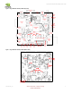
Tegra 200 Series Developer Board User Guide 5.0 THERMAL 5.1 Major Component Thermal Specifications Most of the major components used in Tegra 200 series Developer Board are listed in Table 39 along with the temperature range they are able to operate across.
Tegra 200 Series Developer Board User Guide Figure 27. Top View – Heat Generating and Thermal Sensitive Components Figure 28.
Tegra 200 Series Developer Board User Guide The Tegra 200 Series Developer Board does not represent an actual layout for use in a Smartbook design. It does show the various components typically found in a Smartbook and aids in describing some useful thermal guidelines: Keep hotter or more sensitive components from being in close proximity to each other This may include keeping them from being directly opposite each other on each side of the PCB.
Notice ALL NVIDIA DESIGN SPECIFICATIONS, REFERENCE BOARDS, FILES, DRAWINGS, DIAGNOSTICS, LISTS, AND OTHER DOCUMENTS (TOGETHER AND SEPARATELY, “MATERIALS”) ARE BEING PROVIDED “AS IS.” NVIDIA MAKES NO WARRANTIES, EXPRESSED, IMPLIED, STATUTORY, OR OTHERWISE WITH RESPECT TO THE MATERIALS, AND EXPRESSLY DISCLAIMS ALL IMPLIED WARRANTIES OF NONINFRINGEMENT, MERCHANTABILITY, AND FITNESS FOR A PARTICULAR PURPOSE. Information furnished is believed to be accurate and reliable.