nRF9160 Hardware Integration Guide v1.0 v1.
Contents Revision history. . . . . . . . . . . . . . . . . . . . . . . . . . . . . . . . . . iii 1 About this document. . . . . . . . . . . . . . . . . . . . . . . . . . . . . . 4 2 Device overview. . . . . . . . . . . . . . . . . . . . . . . . . . . . . . . . . 5 2.1 Operating conditions . . . . . . . . . . . . . . . . . . . . . . . . . . . . . . . 2.2 Bands of operation . . . . . . . . . . . . . . . . . . . . . . . . . . . . . . . . 2.3 Supported FCC rules . . . . . . . . . . . . . . . . . . . .
Revision history Date Version Description May 2019 1.0 First release v1.
1 About this document This document complements the nRF9160 Product Specification (PS) to provide recommendations and guidelines for designing devices based on the nRF9160 module. This document is intended for the customers of Nordic Semiconductor, especially system device manufacturers and hardware engineers. v1.
2 Device overview nRF9160 is an LTE made simple cellular IoT System in Package (SiP) module that is pre-certified for customers for building end devices on it. nRF9160 consists of an ARM® Cortex®- M33 microcontroller and 3GPP LTE release 13 compliant embedded Cat-M and Cat-NB LTE modem. The microcontroller has an inbuilt 1 MB flash memory, ARM TrustZone®, and 32 general purpose I/O pins.
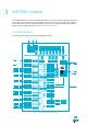
nRF9160 module The nRF9160 SiP module consists of the nRF9160 System on Chip (SoC), power management and RF frontend section, and passive and clocking components. External to the module are supply source (battery or mains), SIM solution, and any customer peripherals and sensors. For further details of blocks and their software controls and dependencies, see nRF9160 Product Specification. 3.1 Block diagram The following block diagram illustrates the nRF9160 SiP module.
nRF9160 module 3.2 Pin assignment The following figure illustrates the nRF9160 pinout. For more information, see Pin assignments in nRF9160 Product Specification. Figure 2: nRF9160 pinout, top (seen through module) 3.3 Pin description Pin descriptions are provided in the following table. The table can be found in Pin assignments in the nRF9160 Product Specification, excluding some information that is relevant for the nRF9160 hardware design.
nRF9160 module Pin no Pin name Function Description 23 P0.13 GPIO Digital I/O and analog input, VDD_GPIO level 24 P0.14 GPIO Digital I/O and analog input, VDD_GPIO level 25 P0.15 GPIO Digital I/O and analog input, VDD_GPIO level 26 P0.16 GPIO Digital I/O and analog input, VDD_GPIO level 27 GND_Shield Power Microshield GND, connect strongly to module GND 28 P0.17 GPIO Digital I/O and analog input, VDD_GPIO level 29 P0.
nRF9160 module Pin no Pin name Function Description 73 Reserved Reserved Can be used to improve mechanical rigidity. Solder to main board but do not 74-82 GND_Shield Power Microshield GND, connect strongly to module GND 83 P0.26 GPIO Digital I/O, VDD_GPIO level 84 P0.27 GPIO Digital I/O, VDD_GPIO level 85 GND_Shield Power Microshield GND, connect strongly to module GND 86 P0.28 GPIO Digital I/O, VDD_GPIO level 87 P0.29 GPIO Digital I/O, VDD_GPIO level 88 P0.
4 Antennas The nRF9160 module supports multiple cellular frequency bands as listed in Bands of operation on page 5. As the electrical size of the antenna sets fundamental limits for antenna bandwidth, it is recommended to select an antenna supporting only the operational bands of the final device and optimize the antenna performance at frequencies in question. The smaller the electrical size, the narrower the reachable bandwidth and the lower the radiation efficiency.
Antennas 4.2 Antenna port test connector To run conductive RF tests, a test connector nearby the nRF9160 antenna port in the RF transmission line is needed. The 50 Ω impedance requirement applies also to the test connector, and VSWR and insertion loss should be minimal. Regardless of whether the nR9160 antenna port is connected to an actual antenna or test equipment, the load at the nRF9160 antenna should remain as close to 50 Ω as possible.
5 Test modes The nRF9160 module is fully calibrated and does not require any calibration in device manufacturer’s production. Instead, the manufacturer test should focus on successful assembly of the module and the peripheral components connected to nRF9160 for correct co-functionality.
Test modes 5.2.1 RX test RX ON command enables the RF receiver with the given parameters. It also measures antenna power with a time domain power meter and returns the measurement result. RX OFF command disables RF receiver.
Test modes Parameter Range Description 3GPP band number 1 to 66 nRF9160 supported bands Frequency 100 kHz raster 6000 to 22000 Corresponds to 600 to 2200 MHz System mode 0 to 1 NB1 = 0, M1 = 1 Signal level at antenna -50 to +23 TX signal level at antenna port [dBm] Modulation CW to 16QAM TX signal properties - options available depending on selected system mode RB or SC count 1 to 12 TX signal properties - options available depending on selected system mode RB or SC start position 0 to
Test modes Parameter Range Description Signal level at antenna -127 to -25 Signal generator level at antenna [dBm] Table 4: GPS SNR ON input parameters The response to the test is GPS SNR value measured by DUT in q4 [dB] format. q4 format results can be converted into dBm value by dividing the result by 2^4 (= 16). Test setup Figure 7: GPS SNR test setup example 5.
6 Reference circuitry To ensure good RF performance when designing PCBs, it is highly recommended to use the PCB layouts and component values provided by Nordic Semiconductor. Documentation for the different package reference circuits, including Altium Designer files, PCB layout files, and PCB production files can be downloaded from www.nordicsemi.com. Note: In this context reference circuitry illustrates the vehicle (i.e.
Reference circuitry Figure 9: nRF9160 reference layout, metal layer 1 (top) Figure 10: nRF9160 reference layout, metal layer 2 6.4 PCB specification The nRF9160 Development Kit PCB stack-up and layer materials are shown in the following figure: v1.
Reference circuitry Figure 11: nRF9160 reference PCB (Elprint’s 4-layer 4001 stack-up) 6.5 Antenna type The antenna used in nRF9160 Development Kit is Ethertronics P822601 shown in the following figure. The antenna is a universal broadband FR4 embedded LTE antenna generally suitable for various cellular applications. Ethertronics’ Universal Broadband Embedded LTE/LPWA antenna utilizes Isolated Magnetic Dipole™ (IMD) technology. For further details on the antenna, see the antenna supplier datasheet. v1.
Reference circuitry Figure 12: nRF9160 Development Kit antenna v1.
7 Regulatory information This section contains information on certified bands and FCC/ISED regulatory notices for nRF9160. 7.1 Certified bands The following table shows the FCC and ISED certified LTE-M1 bands for nRF9160.
Regulatory information 7.2 FCC/ISED regulatory notices FCC/ISED regulatory notices cover modification and interference statements, wireless and FCC Class B digital device notices, permitted antennas and labeling requirements. Modification statement Nordic Semiconductor has not approved any changes or modifications to this device by the user. Any changes or modifications could void the user's authority to operate the equipment.
Regulatory information Type Band Max gain SMD Band 2 9.0 dBi Band 4 6.0 dBi Band 5 7.1 dBi Band 12 6.6 dBi Band 13 6.9 dBi Band 14 6.9 dBi Band 17 6.6 dBi Band 25 9.0 dBi Band 26 7.0 dBi Band 66 6.0 dBi Le présent émetteur radio a été approuvé par ISDE pour fonctionner avec les types d'antenne énumérés ci dessous et ayant un gain admissible maximal.
Regulatory information • Consult the dealer or an experienced radio/TV technician for help CAN ICES-3 (B)/NMB-3 (B) This Class B digital apparatus complies with Canadian ICES-003. Cet appareil numérique de classe B est conforme à la norme canadienne ICES-003. Labeling requirements for the host device The host device shall be properly labelled to identify the modules within the host device.
Legal notices By using this documentation you agree to our terms and conditions of use. Nordic Semiconductor may change these terms and conditions at any time without notice. Liability disclaimer Nordic Semiconductor ASA reserves the right to make changes without further notice to the product to improve reliability, function, or design. Nordic Semiconductor ASA does not assume any liability arising out of the application or use of any product or circuits described herein.