
Installation Guide
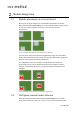
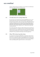
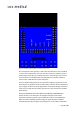
Table Of Contents

Page 6 of 12
Figure 4 Nox Bluetooth LE Module pin numbering (top view)
The assumption is that typically a multi-layer PCB with micro vias is needed,
i.e. micro vias used between the outer top layer where the module is placed
and the signal layer directly under the top layer. One PCB layer of the carrier
board should be a solid GND plane. All GND pads of the module should be
connect with a dedicated via to this GND plane.
Since the module design include all required decoupling capacitors there are
normally not any need for external components, however this may depend on
power supply architecture of the application carrier board design. If external
capacitors are used these should be placed close to the module for best EMI
performance.
Even if the nRF52840 based Nox Bluetooth LE Module (NOXBLEMOD) is
flexible in how to use GPIO pins, the designer should be aware of the
limitations related to general purpose GPIO pins and low speed GPIO pins.
When it comes to PCB design and routing ,the signal integrity should be
considered. Especially the higher speed interfaces, such as SPI or USB, while