
Computer Hardware Installation Guide

Configuring the ESDI card 1097
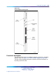
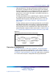
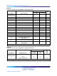
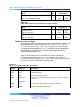
Signal source
Pin number Signal functions To DCE
From
DCE
EIA
circuit
(lead)
Data
2
3
13
16
Transmitted data – lead A
Received data – lead A
Transmitted data – lead B
Received data – lead B
3
—
3
—
—
3
—
3
BA (A)
BB (A)
BA (B)
BB (B)
Control
4
5
6
8
20
Request to send (RTS)
Clear to send (CTS)
Data set ready (DSR)
Carrier detect (CD)
Data terminal ready (DTR)
3
—
—
—
3
—
3
3
3
CA
CB
CC
CF
CD
Timing
12
Transmitter signal element
timing (DTE) – lead B
—
3
DD (B)
14
Transmitter signal element
timing (DCE) – lead B
—
3
DB (B)
15
Transmitter signal element
timing (DCE) – lead A
—
3
DB (A)
17
Transmitter signal element
timing (DTE) – lead A
—
3
DD (A)
23
Receiver signal element timing
(DCE) – lead A
3
—
DA (A)
24
Receiver signal element timing
(DCE) – lead B 3
—
DA (B)
Note: Pins not used are 9, 10, 11, 18, 19, 21, 22, 25.
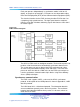
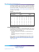
Configuring the ESDI card
Configuring the ESDI card consists of setting the port addresses using the
address selection switch and setting the port interface options using the
jumper blocks. The system software must then be configured to recognize
the ESDI card. Figure 312 "ESDI card option switch locations" (page
1099)shows the location of all option switches and jumper sockets on the
ESDI card.
Address switch settings
The two ESDI ports on the card are addressed in pairs such as 0 and 1, 2
and 3, and so on). The address is set using switch S2. The switch settings
used to select the address vary depending on whether the card is Style A or
Style B. The "Style" can be read on the printed circuit board silk screen. The
address of the card is set to match the device address defined in software.
Nortel Communication Server 1000
Circuit Card Reference
NN43001-311 01.04 Standard
Release 5.0 23 May 2008
Copyright © 2003-2008, Nortel Networks
.