
Datasheet


Revision 1.5 Page 40 of 41
nRF905 Product Specification
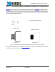
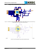
15.4 PCB Layout Example; Single Ended Connection to 50Ω Antenna
Figure 16. shows a PCB layout example for the application schematic in Figure 14. and Figure 17. shows
a PCB layout example for the application schematic in Figure 15.
A double sided FR-4 board of 1.6mm
thickness is used. This PCB has a ground plane on the bottom layer. Additionally, there are ground areas
on the component side of the board to ensure sufficient grounding of critical components. A large number
of via holes connect the top layer ground areas to the bottom layer ground plane.
Figure 16. PCB layout example for 433 MHz operation on nRF905, single ended connection to 50
Ω
antenna by using a differential to single ended matching network
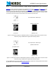
Figure 17. PCB layout example for 868-915 MHz operation on nRF905, single ended connection to 50
Ω
antenna by using a differential to single ended matching network
A fully qualified RF layout for the nRF905 and its surrounding components, including antennas and match-
ing networks, can be downloaded from www.nordicsemi.no
a) Top silk screen
No components in bottom layer
b) Bottom silk screen
c) Top view
d) Bottom view
a) Top silk screen
No components in bottom layer
b) Bottom silk screen
c) Top view
d) Bottom view