
Datasheet


Revision 1.5 Page 30 of 41
nRF905 Product Specification
The application operating frequency must be chosen to apply with the Short Range Device regulation in
the area of operation.
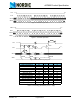
Table 24. Examples of real operating frequencies
11.8 PCB Layout and Decoupling Guidelines
nRF905 is an extremely robust RF device due to internal voltage regulators and requires the minimum of
RF layout protocols. However, the following design rules should still be incorporated into the layout design.
A PCB with a minimum of two layers including a ground plane is recommended for optimum performance.
The DC supply voltage should be decoupled as close as possible to the VDD pins with high performance
RF capacitors. It is preferable to mount a large surface mount capacitor (for example, 4.7µF tantalum) in
parallel with the smaller value capacitors. The supply voltage should be filtered and routed separately from
the supply voltages of any digital circuitry.
Long power supply lines on the PCB should be avoided. All device grounds, VDD connections and VDD
bypass capacitors must be connected as close as possible to the IC. For a PCB with a topside RF ground
plane, the VSS pins should be connected directly to the ground plane. For a PCB with a bottom ground
plane, the best technique is to place via holes as close as possible to the VSS pins. A minimum of one via
hole should be used for each VSS pin.
Full swing digital data or control signals should not be routed close to the crystal or the power supply lines.
A fully qualified RF layout for the nRF905 and its surrounding components, including antennas and match-
ing networks, can be downloaded from www.nordicsemi.no
.
Operating frequency HFREQ_PLL CH_NO
430.0 MHz [0] [001001100]
433.1 MHz [0] [001101011]
433.2 MHz [0] [001101100]
434.7 MHz [0] [001111011]
862.0 MHz [1] [001010110]
868.2 MHz [1] [001110101]
868.4 MHz [1] [001110110]
869.8 MHz [1] [001111101]
902.2 MHz [1] [100011111]
902.4 MHz [1] [100100000]
927.8 MHz [1] [110011111]