
Datasheet


Revision 1.5 Page 29 of 41
nRF905 Product Specification
11.4 Antenna Output
The ANT1 and ANT2 output pins provide a balanced RF output to the antenna. The pins must have a DC
path to VDD_PA, either through a RF choke or through the center point in a dipole antenna. The load
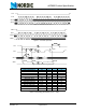
impedance seen between the ANT1/ANT2 outputs should be in the range 200-700W. The optimum differ-
ential load impedance at the antenna ports is given as:
900MHz225
Ω+j210
430MHz300
Ω+j100
A low load impedance (for instance 50
Ω) can be obtained by fitting a simple matching network or a RF
transformer (balun). Further information regarding balun structures and matching networks may be found
in chapter 15 on page 35
.
11.5 Output Power Adjustment
The power amplifier in nRF905 can be programmed to four different output power settings by the configu-
ration register. By reducing output power, the total TX current is reduced.
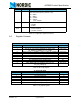
Table 23. RF output power setting for the nRF905
11.6 Modulation
The modulation of nRF905 is Gaussian Frequency Shift Keying (GFSK) with a data rate of 100kbps. Devi-
ation is
±50kHz. GFSK modulation results in a more bandwidth effective transmission link compared with
ordinary FSK modulation.
The data is internally Manchester encoded (TX) and Manchester decoded (RX). That is, the effective sym-
bol rate of the link is 50kbps. By using internally Manchester encoding, no scrambling in the microcontroller
is needed.
11.7 Output Frequency
The operating RF frequency of nRF905 is set in the configuration register by CH_NO and HFREQ_PLL.
The operating frequency is given by:
When HFREQ_PLL is ‘0’ the frequency resolution is 100kHz and when it is ‘1’ the resolution is 200kHz.
Power setting RF output power
DC current
consumption
00 -10 dBm 9.0 mA
01 -2 dBm 14.0 mA
10 6 dBm 20.0 mA
11 10 dBm 30.0 mA
Conditions: VDD = 3.0V, VSS = 0V, T
A
= 27ºC, Load impedance = 400 Ω.
MHzPLLHFREQNOCHf
OP
)_1())10/_(4.422( +⋅+=