
Datasheet


Revision 1.5 Page 26 of 41
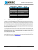
nRF905 Product Specification
10 Important Timing Data
The following timing must be obeyed during nRF905 operation.
10.1 Device Switching Times
Table 21. Switching times for nRF905.
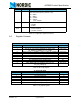
10.2 ShockBurst™ TX timing
Figure 9. Timing diagram for standby to transmit
After a data packet has finished transmitting, the device automatically enters Standby mode and waits for
the next pulse of TRX_CE. If the auto retransmit function is enabled the data packet continues resending
the same data packet until TRX_CE is set low.
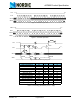
nRF905 timing Max.
PWR_DWN Î ST_BY mode 3 ms
STBY Î TX ShockBurst™ 650 µs
STBY Î RX ShockBurst™ 650 µs
RX ShockBurst™ Î TX ShockBurst™
550 µs
a
a. RX to TX or TX to RX switching is available without re-program-
ming the RF configuration register. The same frequency channel
is maintained.
TX ShockBurst™ Î RX ShockBurst™ 550 µs
MOSI
CSN
PWR_UP
TX_EN
TRX_CE
TX DATA
TIME
T0 = Radio Enabled
T1 = T0+10uS Minimum TRX_CE pulse
T2 = T0 + 650uS.Start of TX Data transmission
T3 = End of Data Packet, enter Standby mode
Programming of
Configuration Register
and TX Data Register
T0 T1
T2 T3
Transmitted Data 100kbps
Manchester Encoded