
Datasheet


Revision 1.5 Page 19 of 41
nRF905 Product Specification
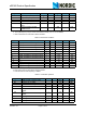
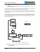
Figure 4. Flowchart ShockBurst™ receive of nRF905.
8.6 Power Down Mode
In power down the nRF905 is disabled with minimal current consumption, typically less than 2.5µA. When
the device enters this mode it is not active which minimizes average current consumption and maximizes
battery lifetime. The configuration word content is maintained during power down.
8.7 Standby Mode
Standby mode is used to minimize average current consumption while maintaining short start up times to
ShockBurst™ RX and ShockBurst™ TX. In this mode part of the crystal oscillator is active. Current con-
sumption is dependent on crystal frequency, Ex: I
DD
= 12µA @4MHz and I
DD
=46µA @20MHz. If the uP-
clock (pin 3) of nRF905 is enabled, current consumption increases and is dependent on the load capaci-
tance and frequency. The configuration word content is maintained during standby.
NO
YES
Receiver is
powered up
NO
YES
Receiving
data
Receiver
Sensing for incomming data
CD is set high if carrier
AM is set
high
NO
DR high is
set high
Radio enters
STBY
MCU clocks out payload via
the SPI interface
DR and AM are
set low
YES
YES
NO
AM is set low
Radio in Standby
TX_EN = LO
PWR_UP = HI
TRX_CE
= HI ?
Correct
ADDR?
Correct
CRC?
TRX_CE
= HI ?
PAYLOAD
Data Packet
ADDR PAYLOAD CRC
Pre-
amble
RX Remains
On
MCU clocks out payload via
the SPI interface
DR and AM are
set low