
Datasheet


Revision 1.5 Page 15 of 41
nRF905 Product Specification
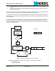
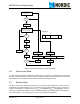
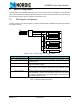
7.2 Pin Functions
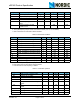
Table 10. nRF905 pin function.
Pin Name Pin function Description
1 TRX_CE Digital input Enables chip for receive and transmit
2 PWR_UP Digital input Power up chip
3 uPCLK Clock output Output clock, divided crystal oscillator full swing clock
4 VDD Power Power supply (+3V DC)
5 VSS Power Ground (0V)
6 CD Digital output Carrier Detect
7 AM Digital output Address Match
8 DR Digital output Receive and transmit Data Ready
9 VSS Power Ground (0V)
10 MISO SPI - interface SPI output
11 MOSI SPI - interface SPI input
12 SCK SPI - Clock SPI clock
13 CSN SPI - enable SPI enable, active low
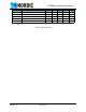
14 XC1 Analog Input Crystal pin 1/ External clock reference pin
15 XC2 Analog Output Crystal pin 2
16 VSS Power Ground (0V)
17 VDD Power Power supply (+3V DC)
18 VSS Power Ground
19 VDD_PA Power output Positive supply (1.8V) to nRF905 power amplifier
20 ANT1 RF Antenna interface 1
21 ANT2 RF Antenna interface 2
22 VSS Power Ground (0V)
23 IREF Analog Input Reference current
24 VSS Power Ground (0V)
25 VDD Power Power supply (+3V DC)
26 VSS Power Ground (0V)
27 VSS Power Ground (0V)
28 VSS Power Ground (0V)
29 VSS Power Ground (0V)
30 VSS Power Ground (0V)
31 DVDD_1V2 Power Low voltage positive digital supply output for decoupling
32 TX_EN Digital input TX_EN=”1”TX mode, TX_EN=”0”RX mode