
Datasheet


Revision 1.5 Page 10 of 41
nRF905 Product Specification
5 Electrical Specifications
Conditions: VDD = +3V VSS = 0V, TEMP = -40ºC to +85ºC (typical +27ºC)
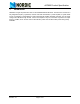
Table 3. Operating conditions
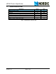
Table 4. Digital input/output
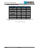
Table 5. Electrical specifications
Symbol Parameter (condition) Notes Min. Typ. Max. Units
VDD Supply voltage 1.9 3.6 V
TEMP Operating temperature -40 85 ºC
Symbol Parameter (condition) Notes Min. Typ. Max. Units
V
IH
HIGH level input voltage 0.7·VDD VDD V
V
IL
LOW level input voltage VSS 0.3·VDD V
Ci Pin capacitance 5 pF
IiL
Pin leakage current
a
a. Max value determined by design and characterization testing.
±10 nA
V
OH
HIGH level output voltage
(I
OH
=-0.5mA)
VDD-0.3 VDD V
V
OL
LOW level output voltage
(I
OL
=0.5mA)
VSS 0.3 V
Symbol Parameter (condition) Notes Min. Typ. Max. Units
I
stby_eclk
Supply current in standby, uCLK
enabled
a
a. Output frequency is 4MHz load of external clock pin is 5pF, Crystal is 4MHz.
100 µA
I
stby_dclk
Supply current in standby, uCLK dis-
abled
b
b. Crystal is 4MHz.
12.5 µA
I
PD
Supply current in power down mode
c
c. Pin voltages are VSS or VDD.
2.5 µA
I
SPI
Supply current in SPI programming
d
d. Chip in power down, SPI_SCK frequency is 1MHz.
20 µA