
Manual


Bank
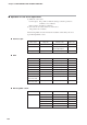
Item name RAM address EEPROM address RAM EEPROM
Decimal point
Remarks
Decimal
Hexadecimal
Decimal
Hexadecimal
Read Write Read Write
information
Instrument
(Reserved for future extension.) 14416 3850 30800 7850 ∆ X ∆ XPSame as RAM address
status 3 7001 (decimal).
(Reserved for future extension.) 14417 3851 30801 7851 ∆ X ∆ X1Same as RAM address
9108 (decimal).
CT (Current transformer) input 1 current
14418 3852 30802 7852 X X 1 Same as RAM address
value 9110 (decimal).
CT (Current transformer) input 2 current
14419 3853 30803 7853 X X 1 Same as RAM address
value 9111 (decimal).
Heat MV (for heat/cool control) 14420 3854 30804 7854 X X 1 Same as RAM address
9106 (decimal).
Cool MV (for heat/cool control) 14421 3855 30805 7855 X X 1 Same as RAM address
9107 (decimal).
Operation LSP group selection 14592 3900 30976 7900 ✽✽— Writing is enabled under no
DI Assignment conditions.
Same as RAM address
9103 (decimal).
LSP value in use 14593 3901 30977 7901 P Same as RAM address
9123 (decimal).
Manual manipulated variable (MV) 14594 3902 30978 7902 ✽✽1 Writing is enabled in the
MANUAL mode.
Same as RAM address
9105 (decimal).
RUN/READY 14595 3903 30979 7903 ✽✽— Writing is enabled under no
DI Assignment conditions.
Same as RAM address
9002 (decimal).
AUTO/MANUAL
14596 3904 30980 7904 ✽✽— Writing is enabled under no
DI Assignment and other
conditions.
Same as RAM address
9001 (decimal).
AT stop/start 14597 3905 30981 7905 ✽✽— Writing is enabled under no
DI Assignment and other
conditions.
Same as RAM address
9004 (decimal).
(Reserved for future extension.) 14598 3906 30982 7906 ∆ X ∆ X—Same as RAM address
9003 (decimal).
PID group P (Proportional band) 14848 3A00 31232 7A00 1
in use I (Integral time) 14849 3A01 31233 7A01 —
D (Derivative time) 14850 3A02 31234 7A02 —
Manual reset 14851 3A03 31235 7A03 1
MV low limit 14852 3A04 31236 7A04 1
MV high limit 14853 3A05 31237 7A05 1
P (Proportional band) (cool) 14854 3A06 31238 7A06 1
I (Integral time) (cool) 14855 3A07 31239 7A07 —
D (Derivative time) (cool) 14856 3A08 31240 7A08 —
(Reserved for future extension.) 14857 3A09 31241 7A09 ∆∆∆∆ 1
Output low limit (Cool) 14858 3A0A 31242 7A0A 1
Output high limit (Cool) 14859 3A0B 31243 7A0B 1
9-12
Chapter 9. LIST OF COMMUNICATION DATA