
Manual


9-10
Chapter 9. LIST OF COMMUNICATION DATA
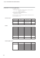
Bank
Item name RAM address EEPROM address RAM EEPROM
Decimal point
Remarks
Decimal
Hexadecimal
Decimal
Hexadecimal
Read Write Read Write
information
Status
Internal Event/Internal Contact control
9203 23F3 25587 63F3 X X — Bits 0 to 4: Internal Event 1
status to 5
Bits 5 to 7: Undefined.
Bits 8 to 10: Internal
Contact 1 to 3
Bits 11 to 15: Undefined.
Control status 9204 23F4 25588 63F4 X X — Bit 0: MANUAL mode
0: AUTO
1: MANUAL
Bit 1: READY mode
0: RUN mode
1: READY mode
Bit 2: Undefined.
Bit 3: During AT
Bit 4: During ST
Bit 5: Undefined.
Bit 6: During SP ramp
Bit 7: During SP up ramp
Bit 8: During SP down ramp
Bits 9 to 12: Undefined.
Bit 13: PID (Heat) is being
used.
Bit 14: PID (Cool) is being
used.
Bit 15: Undefined.
DO status 9205 23F5 25589 63F5 X X — Same as RAM address
14337 (decimal).
Bit 0: Control output 1
Bit 1: Control output 2
Bit 2: Event output 1
Bit 3: Event output 2
Bit 4: Event output 3
Bits 5 to 15: Undefined.
DI status 9206 23F6 25590 63F6 X X — Same as RAM address
14338 (decimal).
Bit 0: DI1
Bit 1: DI2
Bits 3 to 15: Undefined.
Communication DI (DI1 to 4) 9207 23F7 25591 63F7 — Bit 0: Communication DI1
Bit 1: Communication DI2
Bit 2: Communication DI3
Bit 3: Communication DI4
Communication DI1 9208 23F8 25592 63F8 — Bit 0: Communication DI1
Communication DI2 9209 23F9 25593 63F9 — Bit 0: Communication DI2
Communication DI3 9210 23FA 25594 63FA — Bit 0: Communication DI3
Communication DI4 9211 23FB 25595 63FB — Bit 0: Communication DI4
Tag Tag 1 9301 2455 25685 6455 — Display and setting cannot
be made with the console.
Tag 2 9302 2456 25686 6456 — Same as above.
Tag 3 9303 2457 25687 6457 — Same as above.
Tag 4 9304 2458 25688 6458 — Same as above.
Tag 5 9305 2459 25689 6459 — Same as above.
Tag 6 9306 245A 25690 645A — Same as above.
Tag 7 9307 245B 25691 645B — Same as above.
Tag 8 9308 245C 25692 645C — Same as above.
Tag 9 9309 245D 25693 645D — Same as above.
Tag 10 9310 245E 25694 645E — Same as above.
Tag 11 9311 245F 25695 645F — Same as above.