
Manual


Bank
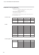
Item name RAM address EEPROM address RAM EEPROM
Decimal point
Remarks
Decimal
Hexadecimal
Decimal
Hexadecimal
Read Write Read Write
information
Operation LSP group selection 9103 238F 25487 638F ✽✽— Same as RAM address
display 14592 (decimal). Writing is
enabled under no DI
Assignment conditions.
(Note 3)
(Reserved for future extension.) 9104 2390 25488 6390 ∆ X ∆ X—
MV (Manipulated Variable) 9105 2391 25489 6391 ✽✽1 Same as RAM address
14594 (decimal). Writing is
enabled in the MANUAL
mode.
Heat MV (Manipulated Variable) 9106 2392 25490 6392 X X 1 Same as RAM address
14420 (decimal).
Cool MV (Manipulated Variable) 9107 2393 25491 6393 X X 1 Same as RAM address
14421 (decimal).
(Reserved for future extension.) 9108 2394 25492 6394 ∆ X ∆ X1Same as RAM address
14417 (decimal).
AT progress 9109 2395 25493 6395 X X —
CT (Current transformer) 9110 2396 25494 6396 X X 1 Same as RAM address
current value 1 14418 (decimal).
CT (Current transformer) 9111 2397 25495 6397 X X 1 Same as RAM address
current value 2 14419 (decimal).
Timer remain time 1 9112 2398 25496 6398 X X S
Timer remain time 2 9113 2399 25497 6399 X X S
Timer remain time 3 9114 239A 25498 639A X X S
Timer remain time 4 9115 239B 25499 639B X X S
Timer remain time 5 9116 239C 25500 639C X X S
(Reserved for future extension.) 9117 239D 25501 639D ∆ X ∆ XS
(Reserved for future extension.) 9118 239E 25502 639E ∆ X ∆ XS
(Reserved for future extension.) 9119 239F 25503 639F ∆ X ∆ XS
(Reserved for future extension.) 9120 23A0 25504 63A0 ∆ X ∆ XS
(Reserved for future extension.) 9121 23A1 25505 63A1 ∆ X ∆ XS
(Reserved for future extension.) 9122 23A2 25506 63A2 ∆ X ∆ XS
LSP value in use 9123 23A3 25507 63A3 P Same as RAM address
14593 (decimal). (Note 2)
PV before ratio, bias, and filter
9124 23A4 25508 63A4 X X P
(Reserved for future extension.) 9125 23A5 25509 63A5 ∆ X ∆ XP
Status Input alarm status 9201 23F1 25585 63F1 X X — Bit 0: AL01 (PV over-range)
Bit 1: AL01 (PV under-
range)
Bit 2: AL03 (CJ, RTD
burnout)
Bits 3 to 15: Undefined.
Instrument alarm status 9202 23F2 25586 63F2 X X — Bits 0 to 1: Undefined.
Bit 2: AL70 (A/D)
Bit 3: AL95 (Set data)
Bit 4: AL96 (Adjustment
data)
Bit 5: AL97 (Set data/RAM)
Bit 6: AL98 (Adjustment
data/RAM)
Bit 7: AL99 (ROM)
Bits 8 to 15 Undefined.
9-9
Chapter 9. LIST OF COMMUNICATION DATA
(Note 2) If the value is read immediately after it has been written into the SP or the LSP in use, the value still may
not be changed. The value is updated after the cycle time has elapsed.
(Note 3) If the SP or the LSP in use is read immediately after the value has been written into the LSP group
selection, the value still may not be changed. The value is updated after the cycle time has elapsed.