
Manual


Bank
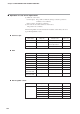
Item name RAM address EEPROM address RAM EEPROM
Decimal point
Remarks
Decimal
Hexadecimal
Decimal
Hexadecimal
Read Write Read Write
information
Event Internal Event 5 main setting 7521 1D61 23905 5D61 S Same as RAM address
13064 (decimal).
Internal Event 5 sub setting 7522 1D62 23906 5D62 S Same as RAM address
13065 (decimal).
Internal Event 5 Hysteresis 7523 1D63 23907 5D63 S
Internal Event 5 ON delay time 7524 1D64 23908 5D64 S
Internal Event 5 OFF delay time 7525 1D65 23909 5D65 S
Extended AT type 8501 2135 24885 6135 —
tuning (Reserved for future extension.) 8502 2136 24886 6136 ∆ X ∆ X—
Just-FiTTER settling band 8503 2137 24887 6137 —
SP lag time 8504 2138 24888 6138 1
(Reserved for future extension.) 8505 2139 24889 6139 ∆ X ∆ X—
AT Proportional band adjust 8506 213A 24890 613A 2
AT Integral time adjust 8507 213B 24891 613B 2
AT Derivative time adjust 8508 213C 24892 613C 2
Control algorithm 8509 213D 24893 613D —
Just-FiTTER overshoot limit/restraint/ 8510 213E 24894 613E —
control coefficient
(Reserved for future extension.) 8511 213F 24895 613F ∆ X ∆ X—
(Reserved for future extension.) 8512 2140 24896 6140 ∆ X ∆ X—
(Reserved for future extension.) 8513 2141 24897 6141 ∆ X ∆ X—
(Reserved for future extension.) 8514 2142 24898 6142 ∆ X ∆ X—
ST (Self-tuning) step execution resolution width
8515 2143 24899 6143 2
ST (Self-tuning) step settling width 8516 2144 24900 6144 2
ST (Self-tuning) hunching settling bound
8517 2145 24901 6145 2
ST (Self-tuning) step ramp change 8518 2146 24902 6146 —
Mode
AUTO/MANUAL
9001 2329 25385 6329 ✽✽—
Same as RAM address
14596 (decimal). Writing is
enabled under no DI
Assignment and other
conditions.
0: AUTO mode
1: MANUAL mode
RUN/READY 9002 232A 25386 632A ✽✽—
Same as RAM address
14595 (decimal). Writing is
enabled under no DI
Assignment conditions
.
0: RUN mode
1: READY mode
(Reserved for future extension.) 9003 232B 25387 632B ∆ X ∆ X—Same as RAM address
14598 (decimal).
AT stop/start 9004 232C 25388 632C ✽✽—
Same as RAM address
14597 (decimal). Writing is
enabled under no DI
Assignment and other
conditions.
0: AT stop
1: AT start
Release all DO latches 9005 232D 25389 632D ✽✽— Writing is enabled under no
DI Assignment conditions.
0: Latch continue
1: Latch release
Operation PV 9101 238D 25485 638D X X P Same as RAM address
display 14356 (decimal).
SP (Target value) 9102 238E 25486 638E P (Note 2)
9-8
Chapter 9. LIST OF COMMUNICATION DATA