
Manual


9-7
Chapter 9. LIST OF COMMUNICATION DATA
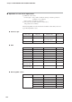
Bank
Item name RAM address EEPROM address RAM EEPROM
Decimal point
Remarks
Decimal
Hexadecimal
Decimal
Hexadecimal
Read Write Read Write
information
SP (Reserved for future extension.) 7001 1B59 23385 5B59 ∆ X ∆ XP
(Reserved for future extension.) 7002 1B5A 23386 5B5A ∆∆∆∆ —
(Reserved for future extension.) 7003 1B5B 23387 5B5B ∆∆∆∆ S
(Reserved for future extension.) 7004 1B5C 23388 5B5C ∆∆∆∆ S
LSP1 7005 1B5D 23389 5B5D P Same as RAM address
13312 (decimal).
(Reserved for future extension.) 7006 1B5E 23390 5B5E ∆∆∆∆ —
(Reserved for future extension.) 7007 1B5F 23391 5B5F ∆∆∆∆ S
(Reserved for future extension.) 7008 1B60 23392 5B60 ∆∆∆∆ S
LSP2 7009 1B61 23393 5B61 P Same as RAM address
13313 (decimal).
(Reserved for future extension.) 7010 1B62 23394 5B62 ∆∆∆∆ —
(Reserved for future extension.) 7011 1B63 23395 5B63 ∆∆∆∆ S
(Reserved for future extension.) 7012 1B64 23396 5B64 ∆∆∆∆ S
LSP3 7013 1B65 23397 5B65 P Same as RAM address
13314 (decimal).
(Reserved for future extension.) 7014 1B66 23398 5B66 ∆∆∆∆ —
(Reserved for future extension.) 7015 1B67 23399 5B67 ∆∆∆∆ S
(Reserved for future extension.) 7016 1B68 23400 5B68 ∆∆∆∆ S
LSP4 7017 1B69 23401 5B69 P Same as RAM address
13315 (decimal).
(Reserved for future extension.) 7018 1B6A 23402 5B6A ∆∆∆∆ —
(Reserved for future extension.) 7019 1B6B 23403 5B6B ∆∆∆∆ S
(Reserved for future extension.) 7020 1B6C 23404 5B6C ∆∆∆∆ S
Event Internal Event 1 main setting 7501 1D4D 23885 5D4D S Same as RAM address
13056 (decimal).
Internal Event 1 sub setting 7502 1D4E 23886 5D4E S Same as RAM address
13057 (decimal).
Internal Event 1 Hysteresis 7503 1D4F 23887 5D4F S
Internal Event 1 ON delay time 7504 1D50 23888 5D50 S
Internal Event 1 OFF delay time 7505 1D51 23889 5D51 S
Internal Event 2 main setting 7506 1D52 23890 5D52 S Same as RAM address
13058 (decimal).
Internal Event 2 sub setting 7507 1D53 23891 5D53 S Same as RAM address
13059 (decimal).
Internal Event 2 Hysteresis 7508 1D54 23892 5D54 S
Internal Event 2 ON delay time 7509 1D55 23893 5D55 S
Internal Event 2 OFF delay time 7510 1D56 23894 5D56 S
Internal Event 3 main setting 7511 1D57 23895 5D57 S Same as RAM address
13060 (decimal).
Internal Event 3 sub setting 7512 1D58 23896 5D58 S Same as RAM address
13061 (decimal).
Internal Event 3 Hysteresis 7513 1D59 23897 5D59 S
Internal Event 3 ON delay time 7514 1D5A 23898 5D5A S
Internal Event 3 OFF delay time 7515 1D5B 23899 5D5B S
Internal Event 4 main setting 7516 1D5C 23900 5D5C S Same as RAM address
13062 (decimal).
Internal Event 4 sub setting 7517 1D5D 23901 5D5D S Same as RAM address
13063 (decimal).
Internal Event 4 Hysteresis 7518 1D5E 23902 5D5E S
Internal Event 4 ON delay time 7519 1D5F 23903 5D5F S
Internal Event 4 OFF delay time 7520 1D60 23904 5D60 S