
User's Manual
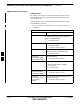


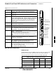
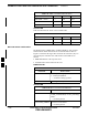

Table Of Contents
- Chapter 4: Acceptance Test Procedures
- Automated Acceptance Test Procedure
- Acceptance Tests - Test Set-up
- Abbreviated (All-inclusive) Acceptance Tests
- Individual Acceptance Tests
- TX Spectral Purity Transmit Mask Acceptance Test
- TX Waveform Quality (Rho) Acceptance Test
- TX Pilot Time Offset Acceptance Test
- TX Code Domain Power/Noise Floor Acceptance Test
- RX FER Acceptance Test
- Generating an ATP Report
- Updating Calibration Data Files
- Chapter 5: Prepare to Leave the Site
- Chapter 6: Troubleshooting
- Basic Troubleshooting: Overview
- Troubleshooting: Installation
- Cannot Log into Cell-Site
- Force LAN A Active (LMF Connection at I/O Panel LAN Connector)
- Force LAN A Active (LMF Connection at Service Shelf LAN Connector)
- Set the GLI IP Address
- Cannot Communicate with Power Meter
- Cannot Communicate with Communications System Analyzer
- Cannot Communicate with Signal Generator
- Troubleshooting: Download
- Troubleshooting: Calibration
- Basic Troubleshooting: RF Path Fault Isolation
- Troubleshooting: Transmit ATP
- Troubleshooting: Receive ATP
- Troubleshooting: CSM Checklist
- Troubleshooting: SCCP Backplane
- Troubleshooting: RFDS
- Module Front Panel LED Indicators and Connectors
- Troubleshooting: Span Control Link
- Appendix A: Data Sheets
- Appendix B: PN Offset/I & Q Offset Register Programming Information
- Appendix C: FRU Optimization / ATP Test Matrix
- Appendix D: BBX Gain Set Point vs. BTS Output
- Appendix E: CDMA Operating Frequency Programming Information
- Appendix F: Test Equipment Preparation
- Test Equipment Preparation
- Verifying and Setting GPIB Addresses
- Agilent E4406A Transmitter Tester GPIB Address
- Agilent E4432B Signal Generator GPIB Address
- Advantest R3267 Spectrum Analyzer GPIB Address
- Advantest R3562 Signal Generator GPIB Address
- Agilent 8935 Series E6380 (formerly HP 8935) Test Set GPIB Address
- Hewlett Packard HP 8921A and HP83236A/B GPIB Address
- Advantest R3465 Communications Test Set GPIB Address
- Motorola CyberTest GPIB Address
- HP 437 Power Meter GPIB Address
- Gigatronics 8541C Power Meter GPIB Address
- RS232 GPIB Interface Adapter
- Test Equipment Inter-Unit Connection, Testing, and Control
- Inter-Unit Connection, Testing, and Control Settings
- HP 8921A with PCS Interface Test Equipment Connections
- HP 8921A with PCS Interface System Connectivity Test
- Pretest Set-up for HP 8921A
- Pretest Set-up for Agilent 8935
- Advantest R3465 Connection
- R3465 GPIB Clock Set-up
- Pretest Set-up for Advantest R3465
- Agilent 8932/E4432B Test Equipment Interconnection
- Agilent E4406A/E4432B Test Equipment Interconnection
- Advantest R3267/R3562 Test Equipment Interconnection
- Equipment Calibration
- Manual Cable Calibration
- Appendix G: Downloading ROM Code
- Appendix H: In-Service Calibration
- Appendix I: Packet Backhaul Configuration
- BTS Router Initial Configuration
- Terminal Setup
- Downloading Minimum Canned BTS Router Configuration Files
- Verifying IOS Canned Version of the CF Memory Card
- Replacing Installed BTS Router CF Memory Card IOS Version
- Background
- Equipment and Software Required for Verification Methods
- Required Publications
- Method 1: Replacement of Installed Router CF Card IOS Data
- Method 2: Using a CF Memory Card Reader for Replacement of Installed IOS Version and Changing File Sequence ...
- Change CF Memory Card File Sequence to Place IOS File First on the Card
- Verify and Upgrade ROMMON Version
- Recovery from BTS Router Boot to ROMMON
- Entering or Changing Router FE Interface IP Address
- Preparation for Site Turn-over
- Index

Module Front Panel LED Indicators and Connectors – continued
FEB 2005 1X SC 4812T Lite BTS Optimization/ATP 6-33
PRELIMINARY
Table 6-35: CSM Card PWR/ALM LED States
LED State Device Status
Solid YELLOW After a reset, the CSMs begin to boot.
Color during the SRAM Test and the Flash
EPROM Code Check Test.
– If SRAM or Flash EPROM Tests fail,
the LED changes to Steady RED and
the CSM attempts to reboot.
OFF 1. No DC Power to the card.
2. The on-board fuse is open.
FREQ Monitor Connector
A Test Port provided on the CSM Front Panel via a BNC Receptacle
allows monitoring of the 19.6608 MHz Clock Signal generated by the
CSM. When both CSM 1 and CSM 2 are in an in-service (INS)
condition, the CSM 2 Clock Signal Frequency is the same as that output
by CSM 1.
The Clock Signal is a Sine Wave Signal with a Minimum Amplitude of
+2 dBm (800 mVpp) into a 50 Ω Load connected to this port.
SYNC Monitor Connector
A Test Port provided at the CSM Front Panel via a BNC Receptacle
allows monitoring of the “Even Second Clock” Reference Signal
generated by the CSM Cards.
At this port, the Reference Signal is a Transistor–Transistor Logic (TTL)
Active–High Signal with a Pulse Width of 153 nanoseconds.
MMI Connector
Behind the Front Panel – only accessible when the card is partially
extended from its SCCP Cage Slot. The RS–232 MMI Port Connector is
intended to be used primarily in the development or factory
environment, but may be used in the field for Debug/Maintenance
purposes.
6