
User's Manual

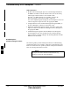
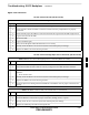
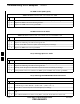


Table Of Contents
- Chapter 4: Acceptance Test Procedures
- Automated Acceptance Test Procedure
- Acceptance Tests - Test Set-up
- Abbreviated (All-inclusive) Acceptance Tests
- Individual Acceptance Tests
- TX Spectral Purity Transmit Mask Acceptance Test
- TX Waveform Quality (Rho) Acceptance Test
- TX Pilot Time Offset Acceptance Test
- TX Code Domain Power/Noise Floor Acceptance Test
- RX FER Acceptance Test
- Generating an ATP Report
- Updating Calibration Data Files
- Chapter 5: Prepare to Leave the Site
- Chapter 6: Troubleshooting
- Basic Troubleshooting: Overview
- Troubleshooting: Installation
- Cannot Log into Cell-Site
- Force LAN A Active (LMF Connection at I/O Panel LAN Connector)
- Force LAN A Active (LMF Connection at Service Shelf LAN Connector)
- Set the GLI IP Address
- Cannot Communicate with Power Meter
- Cannot Communicate with Communications System Analyzer
- Cannot Communicate with Signal Generator
- Troubleshooting: Download
- Troubleshooting: Calibration
- Basic Troubleshooting: RF Path Fault Isolation
- Troubleshooting: Transmit ATP
- Troubleshooting: Receive ATP
- Troubleshooting: CSM Checklist
- Troubleshooting: SCCP Backplane
- Troubleshooting: RFDS
- Module Front Panel LED Indicators and Connectors
- Troubleshooting: Span Control Link
- Appendix A: Data Sheets
- Appendix B: PN Offset/I & Q Offset Register Programming Information
- Appendix C: FRU Optimization / ATP Test Matrix
- Appendix D: BBX Gain Set Point vs. BTS Output
- Appendix E: CDMA Operating Frequency Programming Information
- Appendix F: Test Equipment Preparation
- Test Equipment Preparation
- Verifying and Setting GPIB Addresses
- Agilent E4406A Transmitter Tester GPIB Address
- Agilent E4432B Signal Generator GPIB Address
- Advantest R3267 Spectrum Analyzer GPIB Address
- Advantest R3562 Signal Generator GPIB Address
- Agilent 8935 Series E6380 (formerly HP 8935) Test Set GPIB Address
- Hewlett Packard HP 8921A and HP83236A/B GPIB Address
- Advantest R3465 Communications Test Set GPIB Address
- Motorola CyberTest GPIB Address
- HP 437 Power Meter GPIB Address
- Gigatronics 8541C Power Meter GPIB Address
- RS232 GPIB Interface Adapter
- Test Equipment Inter-Unit Connection, Testing, and Control
- Inter-Unit Connection, Testing, and Control Settings
- HP 8921A with PCS Interface Test Equipment Connections
- HP 8921A with PCS Interface System Connectivity Test
- Pretest Set-up for HP 8921A
- Pretest Set-up for Agilent 8935
- Advantest R3465 Connection
- R3465 GPIB Clock Set-up
- Pretest Set-up for Advantest R3465
- Agilent 8932/E4432B Test Equipment Interconnection
- Agilent E4406A/E4432B Test Equipment Interconnection
- Advantest R3267/R3562 Test Equipment Interconnection
- Equipment Calibration
- Manual Cable Calibration
- Appendix G: Downloading ROM Code
- Appendix H: In-Service Calibration
- Appendix I: Packet Backhaul Configuration
- BTS Router Initial Configuration
- Terminal Setup
- Downloading Minimum Canned BTS Router Configuration Files
- Verifying IOS Canned Version of the CF Memory Card
- Replacing Installed BTS Router CF Memory Card IOS Version
- Background
- Equipment and Software Required for Verification Methods
- Required Publications
- Method 1: Replacement of Installed Router CF Card IOS Data
- Method 2: Using a CF Memory Card Reader for Replacement of Installed IOS Version and Changing File Sequence ...
- Change CF Memory Card File Sequence to Place IOS File First on the Card
- Verify and Upgrade ROMMON Version
- Recovery from BTS Router Boot to ROMMON
- Entering or Changing Router FE Interface IP Address
- Preparation for Site Turn-over
- Index

Troubleshooting: SCCP Backplane – continued
6-24 1X SC 4812T Lite BTS Optimization/ATP FEB 2005
PRELIMINARY
CIO Connectors
S RF RX Antenna Path Signal Inputs are routed through RX Paths of
the DRDCs or TRDCs at the RF Interface Panel (rear of the frame),
and through COAXial Cables to the two MPC Cards.
The three “A” (Main) Signals go to one MPC; the three “B”
(Diversity) Signals to the other. The MPC outputs the
low–noise–amplified signals through the SCCP Backplane to the CIO
where the signals are split and sent to the appropriate BBX.
S A Digital Bus then routes the Baseband Signal through the BBX, to
the SCCP Backplane, and then on to the MCC Slots.
S Digital TX Antenna Path Signals originate at the MCC Cards. Each
output is routed from the MCC Slot through the SCCP Backplane to
the appropriate BBX.
S TX RF Path Signal originates from the BBX, travels through the
SCCP Backplane to the CIO, through the CIO, and then through
multi-conductor COAXial Cabling to the Trunking Module and LPA
Modules in the LPA Shelf.
SCCP Backplane
Troubleshooting Procedure
The following tables provide standard procedures for troubleshooting
problems that appear to be related to a defective SCCP Backplane. The
tables are broken down into possible problems and steps that should be
taken in an attempt to find the root cause.
All steps in all tables should be followed before any
attempt to replace the SCCP Backplane.
NOTE
6