
User's Manual


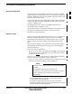

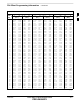
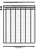


Table Of Contents
- Chapter 4: Acceptance Test Procedures
- Automated Acceptance Test Procedure
- Acceptance Tests - Test Set-up
- Abbreviated (All-inclusive) Acceptance Tests
- Individual Acceptance Tests
- TX Spectral Purity Transmit Mask Acceptance Test
- TX Waveform Quality (Rho) Acceptance Test
- TX Pilot Time Offset Acceptance Test
- TX Code Domain Power/Noise Floor Acceptance Test
- RX FER Acceptance Test
- Generating an ATP Report
- Updating Calibration Data Files
- Chapter 5: Prepare to Leave the Site
- Chapter 6: Troubleshooting
- Basic Troubleshooting: Overview
- Troubleshooting: Installation
- Cannot Log into Cell-Site
- Force LAN A Active (LMF Connection at I/O Panel LAN Connector)
- Force LAN A Active (LMF Connection at Service Shelf LAN Connector)
- Set the GLI IP Address
- Cannot Communicate with Power Meter
- Cannot Communicate with Communications System Analyzer
- Cannot Communicate with Signal Generator
- Troubleshooting: Download
- Troubleshooting: Calibration
- Basic Troubleshooting: RF Path Fault Isolation
- Troubleshooting: Transmit ATP
- Troubleshooting: Receive ATP
- Troubleshooting: CSM Checklist
- Troubleshooting: SCCP Backplane
- Troubleshooting: RFDS
- Module Front Panel LED Indicators and Connectors
- Troubleshooting: Span Control Link
- Appendix A: Data Sheets
- Appendix B: PN Offset/I & Q Offset Register Programming Information
- Appendix C: FRU Optimization / ATP Test Matrix
- Appendix D: BBX Gain Set Point vs. BTS Output
- Appendix E: CDMA Operating Frequency Programming Information
- Appendix F: Test Equipment Preparation
- Test Equipment Preparation
- Verifying and Setting GPIB Addresses
- Agilent E4406A Transmitter Tester GPIB Address
- Agilent E4432B Signal Generator GPIB Address
- Advantest R3267 Spectrum Analyzer GPIB Address
- Advantest R3562 Signal Generator GPIB Address
- Agilent 8935 Series E6380 (formerly HP 8935) Test Set GPIB Address
- Hewlett Packard HP 8921A and HP83236A/B GPIB Address
- Advantest R3465 Communications Test Set GPIB Address
- Motorola CyberTest GPIB Address
- HP 437 Power Meter GPIB Address
- Gigatronics 8541C Power Meter GPIB Address
- RS232 GPIB Interface Adapter
- Test Equipment Inter-Unit Connection, Testing, and Control
- Inter-Unit Connection, Testing, and Control Settings
- HP 8921A with PCS Interface Test Equipment Connections
- HP 8921A with PCS Interface System Connectivity Test
- Pretest Set-up for HP 8921A
- Pretest Set-up for Agilent 8935
- Advantest R3465 Connection
- R3465 GPIB Clock Set-up
- Pretest Set-up for Advantest R3465
- Agilent 8932/E4432B Test Equipment Interconnection
- Agilent E4406A/E4432B Test Equipment Interconnection
- Advantest R3267/R3562 Test Equipment Interconnection
- Equipment Calibration
- Manual Cable Calibration
- Appendix G: Downloading ROM Code
- Appendix H: In-Service Calibration
- Appendix I: Packet Backhaul Configuration
- BTS Router Initial Configuration
- Terminal Setup
- Downloading Minimum Canned BTS Router Configuration Files
- Verifying IOS Canned Version of the CF Memory Card
- Replacing Installed BTS Router CF Memory Card IOS Version
- Background
- Equipment and Software Required for Verification Methods
- Required Publications
- Method 1: Replacement of Installed Router CF Card IOS Data
- Method 2: Using a CF Memory Card Reader for Replacement of Installed IOS Version and Changing File Sequence ...
- Change CF Memory Card File Sequence to Place IOS File First on the Card
- Verify and Upgrade ROMMON Version
- Recovery from BTS Router Boot to ROMMON
- Entering or Changing Router FE Interface IP Address
- Preparation for Site Turn-over
- Index

PN Offset Programming Information
FEB 2005 1X SC 4812T Lite BTS Optimization/ATP B-1
PRELIMINARY
PN Offset Background
All Channel Elements transmitted from a BTS in a specific 1.25 MHz
CDMA Channel are orthogonally spread by 1 of 64 possible Walsh Code
Functions; additionally, they are also spread by a Quadrature Pair of PN
Sequences unique to each sector.
Overall, the mobile uses this to differentiate multiple signals transmitted
from the same BTS (and surrounding BTS) Sectors, and to synchronize
to the next strongest sector.
The PN Offset per Sector is stored on the BBX Cards, where the
corresponding I and Q Registers reside.
The PN Offset Values are determined by BTS Sector (Antenna) based on
the applicable CDF Data Field Content. A breakdown of this
information is found in Table B-1.
PN Offset Usage
There are three basic RF Chip Delays currently in use. It is important to
determine which RF Chip Delay is valid to be able to test the BTS
Functionality. This can be done by ascertaining if the CDF FineTxAdj
Value was set to “on” when the MCC was downloaded with “image
data”.
The
FineTxAdj Value is used to compensate for the Processing Delay
(approximately 20 mS) in the BTS using any type of mobile meeting
IS–97 Specifications.
Observe the following guidelines:
S If the FineTxAdj Value in the CDF is 101 (65 HEX), the FineTxAdj
has not been set. The I and Q Values from the 0 Chip Delay Column
of Table B-1 MUST be used.
If the
FineTxAdj Value in the CDF File is 213 (D5 HEX), FineTxAdj
has been set for the 14 Chip Delay column of Table B-1.
S If the FineTxAdj value in the CDF File is 197 (C5 HEX), FineTxAdj
has been set for the 13Chip Delay column of Table B-1.
CDF File I and Q Values can be represented in DECIMAL
or HEX.
If using HEX, add 0x before the HEX Value.
If necessary, convert HEX values in Table B-1 to decimal
before comparing them to CDF File I and Q Value
Assignments.
NOTE
– If a Qualcomm Mobile is used, select I and Q Values from the
13–Chip Delay column of Table B-1.
– If a mobile is used that does not have the “One Chip Offset”
problem (any mobile meeting the IS–97 Specification), select from
the 14–Chip Delay column of Table B-1.
B